Spartan-6 FPGA PCB Design and Pin Planning www.xilinx.com 55
UG393 (v1.1) April 29, 2010
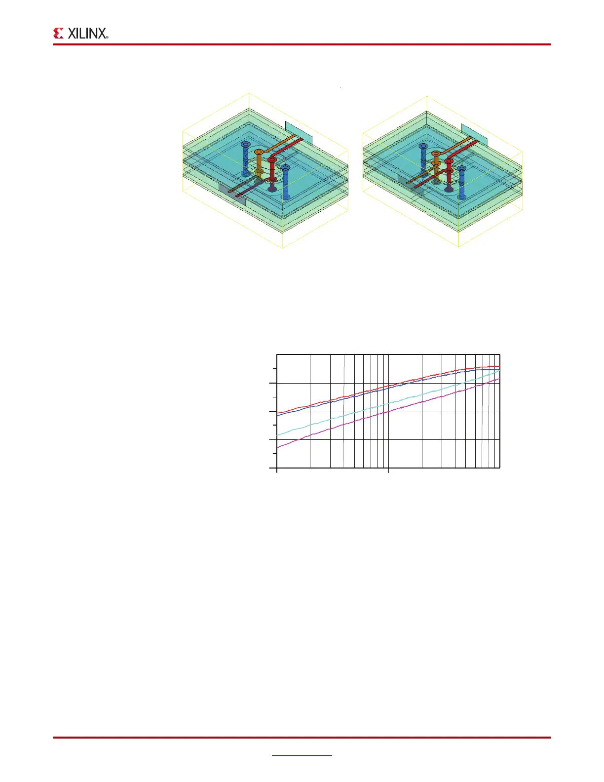
Differential Vias
As a general rule, the P and N paths need to be kept at equal lengths through a transition.
Where possible, via stub length should be kept to a minimum by traversing the signal
through the entire length of the vias. The analysis shown in Figure 5-15 compares the
S-parameter return loss for common-mode (SCC11) and differential (SDD11) responses.
From the graph in Figure 5-15, the common-mode response is 20 dB worse in terms of
return loss. The much worse common-mode response relative to the differential response
is the reason why it is a good idea to reduce P/N skew as much as possible before entering
a transition. The 60/40 rule of thumb is 40 dB of return loss at 1 GHz, which implies 60 fF
of excess capacitance. Because excess capacitance is a single pole response, simple
extrapolation rules can be used. For example, a shift to 34 dB return loss doubles the excess
capacitance. Due to the excellent performance characteristics of GSSG vias, even long via
stubs only double the differential via’s capacitance at the most.
X-Ref Target - Figure 5-14
Figure 5-14: Differential GSSG Via in 16-Layer PCB from Pins L11 and L6
X-Ref Target - Figure 5-15
Figure 5-15: Simulated Return Loss Comparing Differential and Common-Mode
Losses for L11 and L6 GSSG Vias
UG393_c5_14_091809
From Pin L11, Exiting at Lower Layer From Pin L6, Exiting at Middle Layer
UG393_c5_15_091809
1E91E8 1E10
-60
-40
-20
-80
0
Frequency, Hz
dB(Scc11_L11)
dB(Scc11_L6)
dB(Sdd11_L11)
dB(Sdd11_L6)

 Loading...


