33
ABOV Semiconductor Co., Ltd.
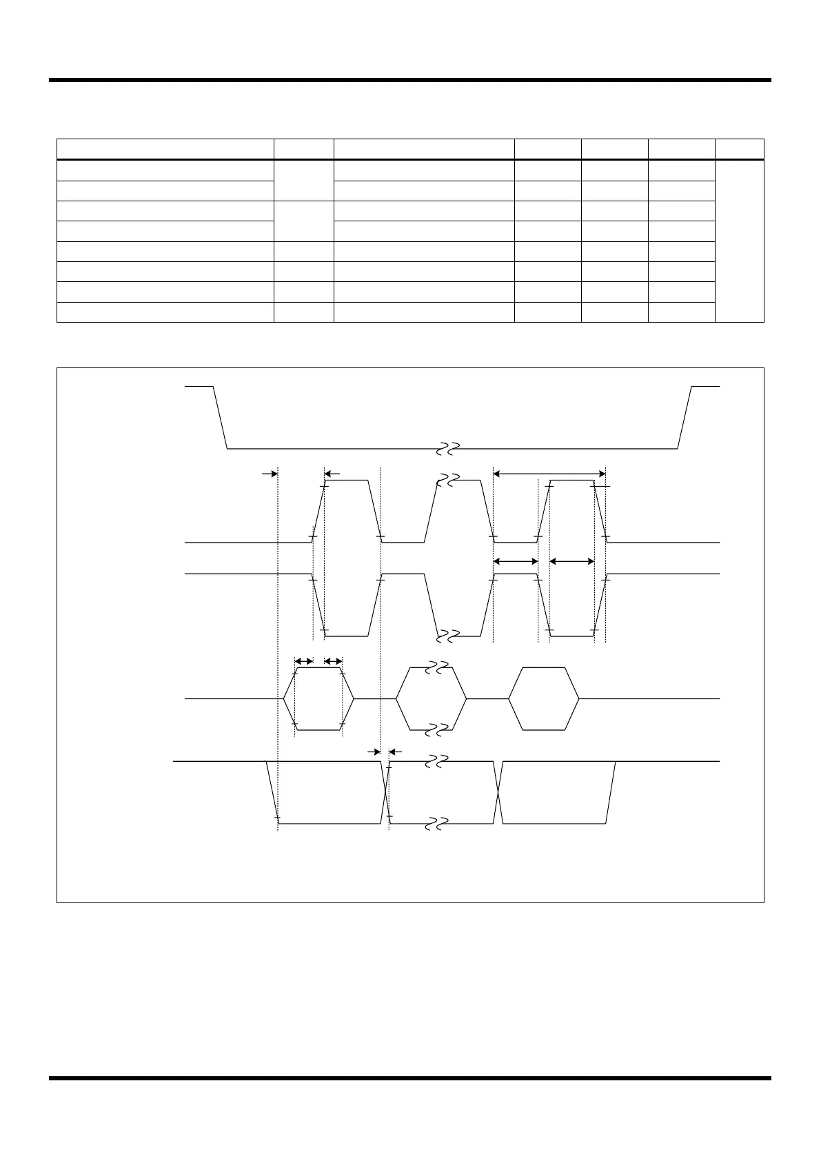
7.11 SPI0/1/2 Characteristics
(T
A
=-40°C– +85°C, VDD=1.8V – 5.5V)
Output Clock Pulse Period
Output Clock High, Low Pulse Width
Input Clock High, Low Pulse Width
First Output Clock Delay Time
Internal/External SCK source
Table 7.12 SPI0/1/2 Characteristics
SSn
(Output/Input)
SCKn
(CPOLn=0)
(Output/Input)
SCKn
(CPOLn=1)
(Output/Input)
MISOn/MOSIn
(Data Input)
tFOD
tSCK
tSCKL tSCKH
0.8VDD
0.2VDD
MSB LSB
tDIS tDIH
MISOn/MOSIn
(Data Output)
MSB LSB
tDS
Figure 7.2 SPI0/1/2 Timing

 Loading...


