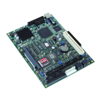
SBC-GX1 Technical Manual Detailed hardware description
runs at 75MHz PC100 memory should be used. If the bus runs at 100MHz then PC133
memory should be used.
The CAS latency can also have a large effect on performance of the board. The board
can support modules with a latency of 2 or 3 clocks. The clock divider and CAS latency
settings are altered in the
Chipset features setup screen within the Setup utility (see
page 34
). The default values select a bus speed of 75MHz and CAS latency is
automatically detected by the BIOS.
The memory timings cannot be changed if the board is using the General
Software BIOS. The timings are fixed and the board is configured for operation
at 75MHZ with a CAS latency of 3.
BIOS EPROM
A 256K byte Flash EPROM device is used to store the BIOS code. This device can be
reprogrammed in situ. using the FLASHROM utility supplied on the support CD (See
the software support section for details). The BIOS stored in this device is compressed
to save space and is uncompressed during the power up process. The system BIOS is
copied into shadow RAM between 0E0000H and 0FFFFFH and the VGA BIOS is
copied to 0C0000H.
The flash device is a +5V only device and there are no link settings required to enable
programming.
Flash memory
The SBC-GX1 board supports up to 16MB flash memory. This memory is configured to
be a read/write silicon disk drive. The Datalight FlashFX flash filling system is
automatically loaded during the POST routine to enable the flash drive to be accessed.
The flash drive uses a 16K memory window at 000DC000-000DFFFFH to access the
devices and two I/O address locations are used to select the appropriate flash area.
Under normal circumstances the Flash FX driver should be used to access this
memory. The FLASH status LED illuminates whenever the Flash drive is accessed.
The I/O registers are shown on the next page for information.
© 2004 Arcom Issue D 64

 Loading...