5.1.2 JTAG 20 connector
The MPS2 and MPS2+ FPGA Prototyping Boards each provide one 3V 20-pin IDC connector that
supports P-JTAG processor debug to enable connection of DSTREAM or a compatible third-party
debugger. The connector also supports SWD.
The JTAG 20 connector connects to general‑purpose pins on the FPGA. The availability of P-JTAG or
SWD depends on the design which you implement in the FPGA. The MPS2 and MPS2+ FPGA
Prototyping Boards label this connector as PJTAG.
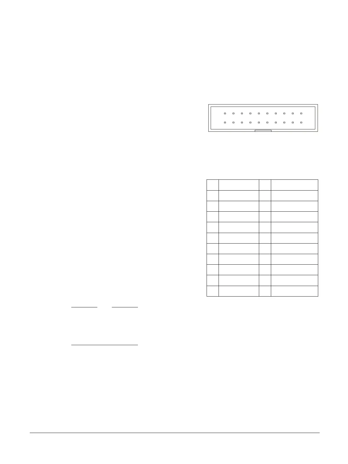
The following figure shows the JTAG 20 connector.
1 19
2 20
Figure 5-2 JTAG 20 connector
The following table shows the pin mapping for each SWD and P-JTAG signal on the JTAG 20 connector
J4.
Table 5-2 JTAG 20 connector, J4, signal list
Pin Signal Pin Signal
1 3V0_OUT 2 3V0_OUT -optional
3 nTRST 4 GND
5 TDI 6 GND
7 SWDIO/TMS 8 GND
9 SWDCLK/TCK 10 GND
11 GND/RTCK 12 GND
13 SWO/TDO 14 GND
15 nSRST 16 GND
17 NC/DBGRQ 18 GNDDETECT
19 NC/DBGACK 20 GND
Note
• The MPS2 and MPS2+ FPGA Prototyping Boards do not support adaptive clocking. The boards tie
the RTCK signal low.
• Pins 3, 5, 7, 13, 15 and 18 have pullup resistors to 3V.
• Pin 9 has a pulldown resistor to GND.
Related information
2.15.3 P-JTAG on page 2-45
2.15.6 Serial Wire Debug on page 2-45
1.3 Location of components on the MPS2 FPGA Prototyping Board on page 1-17
1.4 Location of components on the MPS2+ FPGA Prototyping Board on page 1-19
5.1.3 CoreSight 10 connector
The MPS2 and MPS2+ FPGA Prototyping Boards provide one 3V 10-pin IDC connector. This connector
supports P-JTAG processor debug to enable connection of DSTREAM or a compatible third-party
debugger. This connector also supports SWD.
5 Signal Descriptions
5.1 Debug connectors
100112_0200_09_en Copyright © 2013–2016, 2018–2020 Arm Limited or its affiliates. All
rights reserved.
5-76
Non-Confidential