3B1
2-2-1
2-2-1 Fax control PCB
Add-on memory
CN4
Data bus
Address bus
BUBAT
CN6
CN3
CN1
CN8
+12V DC
+5V DC
CPU
ASIC
Lithium
battery
BT101
PSPCB
Back up
circuit 2
Back up
circuit 1
RTC
LVC
LVC
LVC
LVC
CPU
IC11
ASIC
IC71
SDRAM
IC21
28.224MHz
Modem
LSI
IC81
FLASH
ROM
IC51,52
CG
ROM
IC61
SRAM
IC62
IC63
Analog circuit
Telephone
line
Flash tool
NCUPCB
MPCB
CN5
8-bit
16-bit 16-bit 32-bit 32-bit 32-bit
32-bit
Crystal
oscillator
Clock driver
IC12
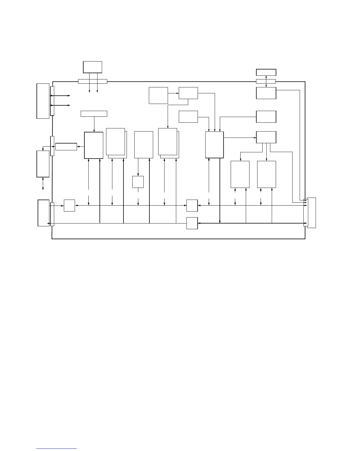
Figure 2-2-1 Fax control PCB block diagram
The fax control PCB (FCPCB) controls the overall fax operation.
To transmit a fax, image data scanned by the optical section of the copier is processed by the main PCB (MPCB) and then
sent to the fax control PCB (FCPCB). Received image data is first stored in the bitmap area of the SDRAM IC21 page by
page and compressed using the MH, MR or MMR method. The data is then stored in the image memory area of the SDRAM
IC21 and sent to the modem LSI IC81 to be modulated from digital signal to analog signal before it is sent to the telephone
line via the NCU PCB (NCUPCB).
To receive a fax, analog image data received from the telephone line via the NCU PCB (NCUPCB) is sent to the modem LSI
IC81 and, after demodulation into digital signals, stored in the image memory area of the SDRAM IC21. The image data is
then decompressed and converted into the bitmap area of the SDRAM IC21 page by page and sent to the ASIC IC71 for
resolution conversion and smoothing, and is passed to the main PCB (MPCB) as print image data.
 Loading...