3B1
2-2-11
2-2-4 Auxiliary power source PCB
5.2 V DC
D5
T1
D2
AC input
Q2
C7
C19
+
+
D6
Relay
PC1
C15,91
C20
GND
GND
Relay REM
DC12V
Overvoltage
detection circuit
12 V DC
output circuit
IC2
5.2 V DC
output
circuit
IC1
Switching
control circuit
PSPCB
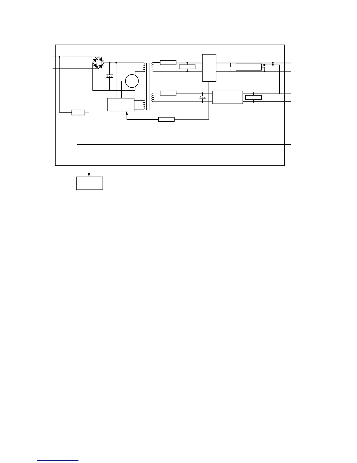
Figure 2-2-7 Auxiliary power source PCB block diagram
The auxiliary power source PCB (APSPCB) is a switching regulator that converts an AC input to generate 5.2 V DC and 12
V DC. It consists of a switching control circuit, 5.2 V DC output circuit and 12 V DC output circuit.
The rectifier circuit rectifies the full-wave of the AC input using the diode bridge D2. The smoothing capacitor C7 smoothes
out the pulsed current from the diode bridge.
The switching control circuit turns on/off the power MOSFET Q2 with the voltage induced in the controlling coil of the
transformer T1 to switch the current induced in the primary coil of the transformer T1.
The 5.2 V DC output circuit smoothes out the voltage from the current induced in the secondary coil of the transformer T1
via the diode D5 and smoothing capacitors C15 and C91, and outputs a stable 5.2 V DC using the shunt regulator IC1. The
output status of the 5.2 V DC is fed back to the switching control circuit via the photo-coupler PC1. Based on the feedback,
the switching control circuit changes the duty cycle of the pulse that turns power MOSFET Q2 on/off in order to adjust the
5.2 V DC.
The 12 V DC output circuit smoothes out voltage from the current induced in the secondary coil of the transformer T1 via the
diode D6 and smoothing capacitor C19, and generates a stable 12 V DC using the 3-pin regulator IC2.
The relay turns on/off the AC supply to the power source PCB (PSPCB) based on the remote signal from the fax control
PCB (FCPCB).


 To Next Page