24
2.7.3 PCS Module Front Panel
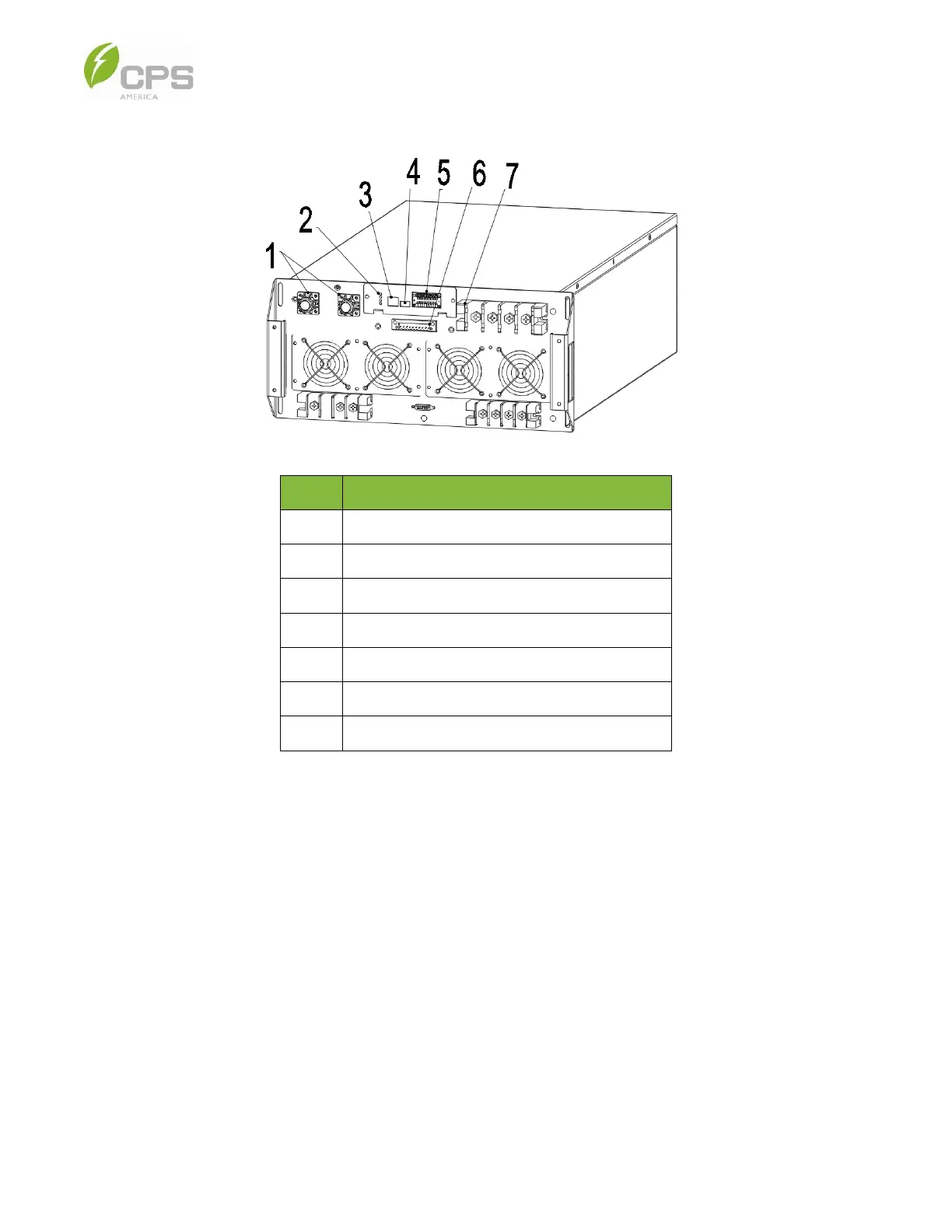
Figure 2-9 Module Appearance (62.5 kW Primary Only)
No. Item
1 DC terminals
2 LED indicator
3 Ethernet port
4
USB port
5
RS485 / CAN / RS232 terminal
6
24 V input and output, dry contacts
7
AC terminals
2.7.4 PCS Schematic Diagram and Circuit Design
The basic electrical schematic diagram of the CPS ECB62.5KTL-M inverter is shown below (Figure 2-10). The DC input from
the batteries connects to the DC side of the PCS inverter, passes through the DC contactor, then converts to the three-phase
AC waveform through three-level inverting technology. The high frequency harmonic distortion is removed with an output filter
and the output AC goes through the AC contactors.