LX-300+/1170 Revision C
PRODUCT DESCRIPTION Interface Specifications 22
o
BUSY signal is active (HIGH level) under the conditions below:
n
In the process of receiving data
n
In the condition of being input buffer full
n
In the condition of being -INT signal active (low level)
n
During hardware initialization
n
In the condition of being -ERROR or PE signal is active (low level, high level,
respectively)
n
In the self test mode
n
In the adjustment mode
n
In the default-setting mode
o -ERROR signal is active (low level) under the conditions below:
n
In the condition of a paper-out error
n
In the condition of a release lever error
o PE signal is active (high level) under the condition below:
n
In the condition of a paper-out error
NOTE: In/Out shows the direction of signal flow from the printer’s point of view.
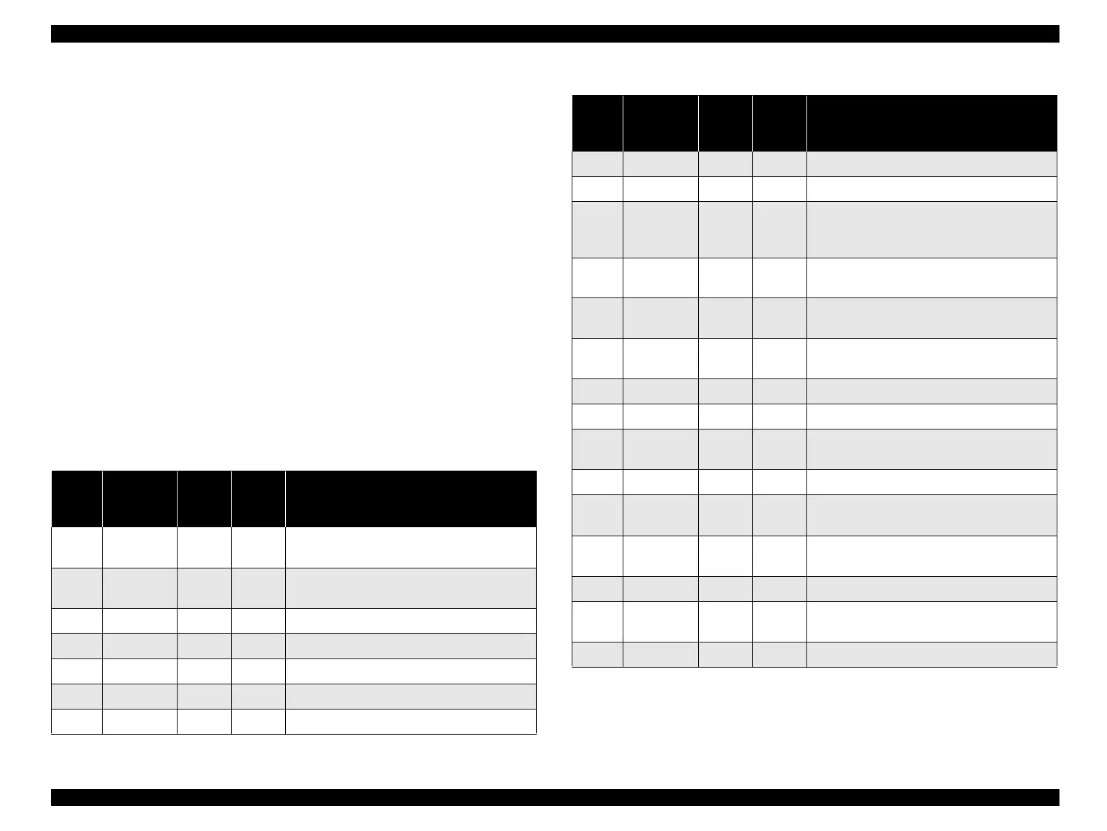
Table 1-12. Connector Pin Assignment and Signals (Forward Channel)
Pin No.
Signal
Name
Return
GND
Pin
In/Out Functional Description
1 -STROBE 19 In
Strobe pulse. Input data is latched at falling
edge of the signal.
2 DATA1 20 In
Parallel input data to the printer.
bit0:LSB
3 DATA2 21 In bit1
4 DATA3 22 In bit2
5 DATA4 23 In bit3
6 DATA5 24 In bit4
7 DATA6 25 In bit5
8 DATA7 26 In bit6
9 DATA8 27 In bit7:MSB
10 -ACKNLG 28 Out
This signal (negative pulse) indicates that the
printer has received data and is ready to accept
next one.
11 BUSY 29 Out
This signal’s high level means that the print is
not ready to accept data.
12 PE 28 Out
This signal’s high level means that the printer is
in a state of paper-out error.
13 SLCT 28 Out
Always at high level when the printer is
powered on.
14 -AFXT 30 In Not used.
31 -INIT 30 In This signal’s negative pulse initializes printer.
32 -ERROR 29 Out
This signal’s low level means the printer is in a
state of error.
36 -SLIN 30 In Not used.
18 Logic H -- Out
This line is pulled up to +5V through
3.9 kΩ resister.
35 +5V -- Out
This line is pulled up tp +5V through
1.0 kΩ resister.
17 Chassis -- -- Chassis GND.
16, 33,
19-30
GND -- -- Signal GND.
15, 34 NC -- -- Not connected.
Table 1-12. Connector Pin Assignment and Signals (Forward Channel)
Pin No.
Signal
Name
Return
GND
Pin
In/Out Functional Description
 Loading...