QUEUED SERIAL MODULE MC68332
6-6 USER’S MANUAL
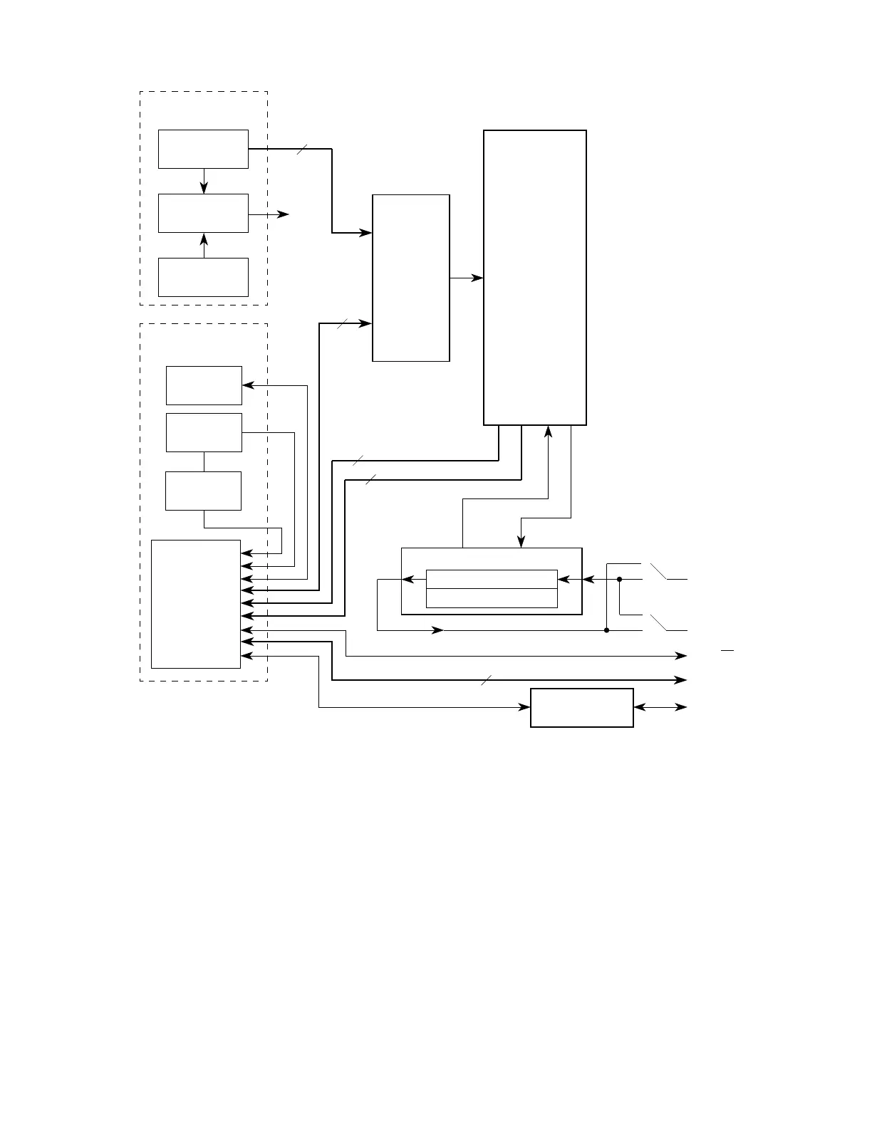
Figure 6-2 QSPI Block Diagram
6.3.1 QSPI Registers
The programmer's model for the QSPI consists of the QSM global and pin control reg-
isters, four QSPI control registers (SPCR[0:3]), a status register (SPCR), and the 80-
byte QSPI RAM.
Registers and RAM can be read and written by the CPU. Refer to APPENDIX D REG-
ISTER SUMMARY for register bit and field definitions.
QSPI BLOCK
CONTROL
REGISTERS
END QUEUE
POINTER
QUEUE
POINTER
STATUS
REGISTER
DELAY
COUNTER
COMPARATOR
PROGRAMMABLE
LOGIC ARRAY
80-BYTE
QSPI RAM
CHIP SELECT
COMMAND
DONE
4
4
3
BAUD RATE
GENERATOR
PCS [3:1]
PCS0/SS
MISO
MOSI
SCK
M
S
M
S
8/16-BIT SHIFT REGISTER
Rx/Tx DATA REGISTER
MSB LSB
4
QUEUE CONTROL
BLOCK
CONTROL
LOGIC
ADDRESS
REGISTER
4
Fr
ees
cale S
em
iconduct
or
, I
Freescale Semiconductor, Inc.
For More Information On This Product,
Go to: www.freescale.com
nc...