MC68332 SYSTEM INTEGRATION MODULE
USER’S MANUAL 4-43
4.6.5.2 Reset States of Pins Assigned to Other MCU Modules
As a rule, module pins that are assigned to general-purpose I/O ports go to active high-
impedance state following reset. Other pin states are determined by individual module
control register settings. Refer to sections concerning modules for details. However,
during power-up reset, module port pins may be in an indeterminate state for a short
period. Refer to 4.6.7 Power-On Reset for more information.
4.6.6 Reset Timing
The RESE
T input must be asserted for a specified minimum period for reset to occur.
External RESET
assertion can be delayed internally for a period equal to the longest
bus cycle time (or the bus monitor time-out period) in order to protect write cycles from
being aborted by reset. While RESET
is asserted, SIM pins are either in an inactive,
high impedance state or are driven to their inactive states.
When an external device asserts RESET for the proper period, reset control logic
clocks the signal into an internal latch. The control logic drives the RESET
pin low for
an additional 512 CLKOUT cycles after it detects that the RESET
signal is no longer
being externally driven, to guarantee this length of reset to the entire system.
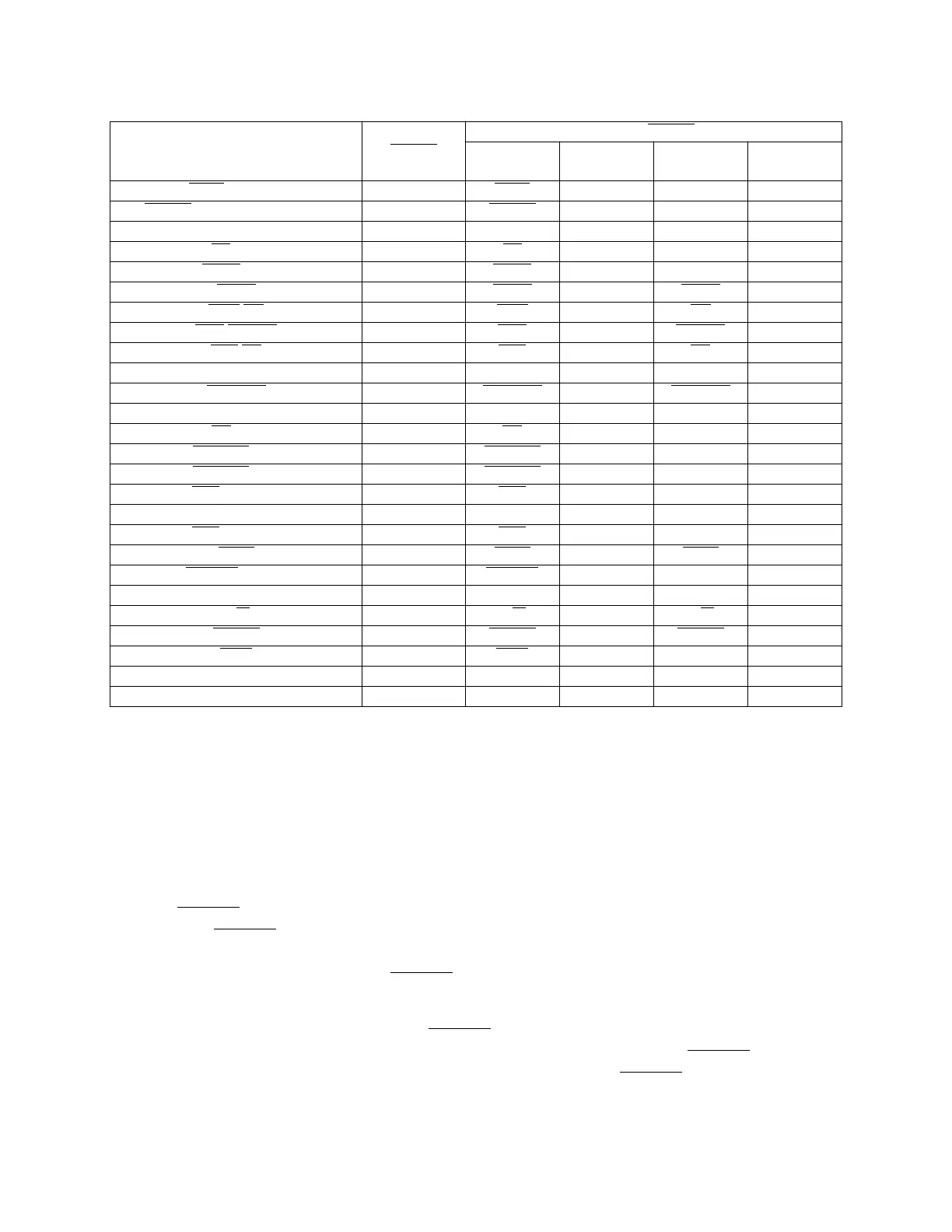
Table 4-18 SIM Pin Reset States
State While Pin State After RESET Released
Mnemonic RESET
Asserted
Pin
Function
Pin State Pin
Function
Pin State
CS10
/ADDR23 1 CS10 1 ADDR23 Unknown
CS[9:6]
/ADDR[22:19]/PC[6:3] 1 CS[9:6] 1 ADDR[22:19] Unknown
ADDR[18:0] High-Z Output ADDR[18:0] Unknown ADDR[18:0] Unknown
AS
/PE5 High-Z Output AS Output PE5 Input
AVEC
/PE2 Disabled AVEC Input PE2 Input
BERR
Disabled BERR Input BERR Input
CSM
/BG 1 CSM 1BG1
CSE
/BGACK 1 CSE 1 BGACK Input
CS0
/BR 1 CS0 1BRInput
CLKOUT Output CLKOUT Output CLKOUT Output
CSBOOT
1 CSBOOT 0 CSBOOT 0
DATA[15:0] Mode Select DATA[15:0] Input DATA[15:0] Input
DS
/PE4 Disabled DS Output PE4 Input
DSACK0
/PE0 Disabled DSACK0 Input PE0 Input
DSACK1
/PE1 Disabled DSACK1 Input PE1 Input
CS5
/FC2/PC2 1 CS5 1 FC2 Unknown
FC1/PC1 1 FC1 1 FC1 Unknown
CS3
/FC0/PC0 1 CS3 1 FC0 Unknown
HALT
Disabled HALT Input HALT Input
IRQ[7:1]
/PF[7:1] Disabled IRQ[7:1] Input PF[7:1] Input
MODCLK/PF0 Mode Select MODCLK Input PF0 Input
R/W
Disabled R/W Output R/W Output
RESET
Asserted RESET Input RESET Input
RMC
Disabled RMC Output PE3 Input
SIZ[1:0]/PE[7:6] Disabled SIZ[1:0] Unknown PE[7:6] Input
TSC Mode Select TSC Input TSC Input
Fr
ees
cale S
em
iconduct
or
, I
Freescale Semiconductor, Inc.
For More Information On This Product,
Go to: www.freescale.com
nc...
 Loading...