MC68332 REGISTER SUMMARY
USER’S MANUAL D-37
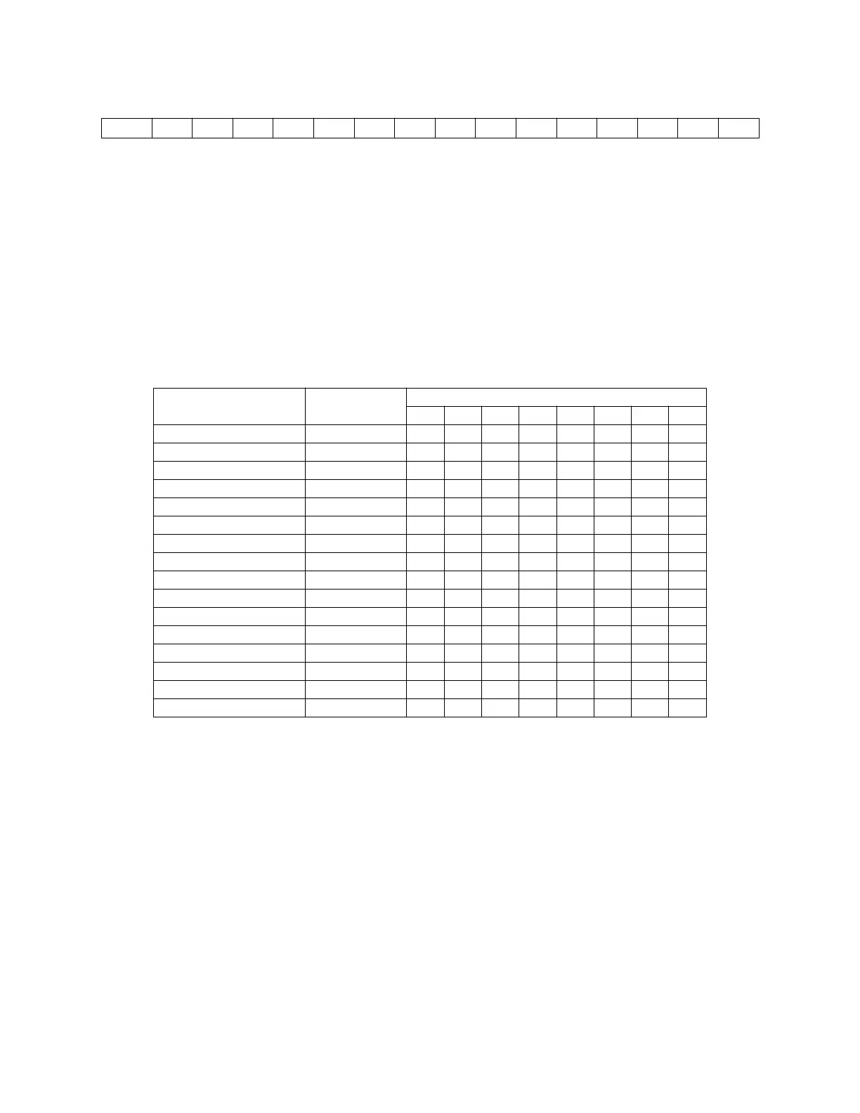
D.5.20 DCNR — Decoded Channel Number Register $YFFE26
CH[15:0] — Service Status Bits
D.5.21 TPU Parameter RAM
The channel parameter registers are organized as one hundred 16-bit words of RAM.
Channels 0 to 13 have six parameters. Channels 14 and 15 each have eight parame-
ters. The parameter registers constitute a shared work space for communication be-
tween the bus master and the TPU.
Y = M111, where M is the logic state of the module mapping (MM) bit in the SIMCR.
15 14 13 12 11 10 9 8 7 6 5 4 3 2 1 0
CH 15 CH 14 CH 13 CH 12 CH 11 CH 10 CH 9 CH 8 CH 7 CH 6 CH 5 CH 4 CH 3 CH 2 CH 1 CH 0
RESET:
0 0 0 0 0 0 0 0 0 0 0 0 0 0 0 0
Table D-6 Parameter RAM Address Map
Channel Base Parameter
Number Address 01234567
0 $YFFF## 00 02 04 06 08 0A — —
1 $YFFF## 10 12 14 16 18 1A — —
2 $YFFF## 20 22 24 26 28 2A — —
3 $YFFF## 30 32 34 36 38 3A — —
4 $YFFF## 40 42 44 46 48 4A — —
5 $YFFF## 50 52 54 56 58 5A — —
6 $YFFF## 60 62 64 66 68 6A — —
7 $YFFF## 70 72 74 76 78 7A — —
8 $YFFF## 80 82 84 86 88 8A — —
9 $YFFF## 90 92 94 96 98 9A — —
10 $YFFF## A0 A2 A4 A6 A8 AA — —
11 $YFFF## B0 B2 B4 B6 B8 BA — —
12 $YFFF## C0 C2 C4 C6 C8 CA — —
13 $YFFF## D0 D2 D4 D6 D8 DA — —
14 $YFFF## E0 E2 E4 E6 E8 EA EC EE
15 $YFFF## F0 F2 F4 F6 F8 FA FC FE
Fr
ees
cale S
em
iconduct
or
, I
Freescale Semiconductor, Inc.
For More Information On This Product,
Go to: www.freescale.com
nc...