MC68332 OVERVIEW
USER’S MANUAL 3-7
3.4 Signal Descriptions
The following tables define MCU signals. Table 3-4 shows signal origin, type, and ac-
tive state. Table 3-5 describes signal functions. Both tables are sorted alphabetically
by mnemonic. MCU pins often have multiple functions. More than one description can
apply to a pin.
NOTES:
1. DATA[15:0] are synchronized during reset only. MODCLK is synchronized only when used as an input port pin.
2. EXTAL, XFC, and XTAL are clock reference connections.
TXD Bo Y Y I/O PQS7
XFC
2
— — — Special —
XTAL
2
— — — Special —
Table 3-3 MCU Power Connections
Pin Mnemonic Description
V
STBY
Standby RAM Power
V
DDSYN
Clock Synthesizer Power
V
SSE
/V
DDE
External Periphery Power (Source and Drain)
V
SSI
/V
DDI
Internal Module Power (Source and Drain)
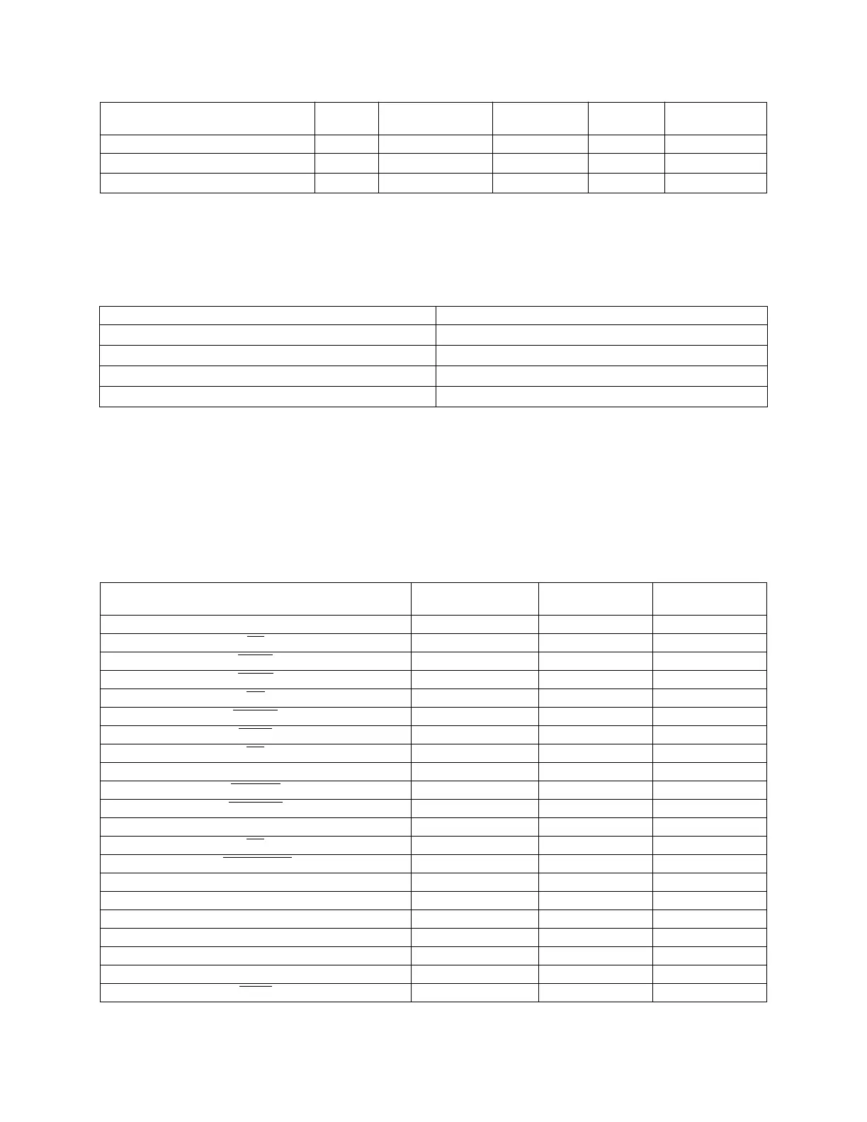
Table 3-4 MCU Signal Characteristics
Signal
Name
MCU
Module
Signal
Type
Active
State
ADDR[23:0] SIM Bus —
AS
SIM Output 0
AVEC
SIM Input 0
BERR
SIM Input 0
BG
SIM Output 0
BGACK
SIM Input 0
BKPT
CPU32 Input 0
BR
SIM Input 0
CLKOUT SIM Output —
CS[10:0]
SIM Output 0
CSBOOT
SIM Output 0
DATA[15:0] SIM Bus —
DS
SIM Output 0
DSACK[1:0]
SIM Input 0
DSCLK CPU32 Input Serial Clock
DSI CPU32 Input (Serial Data)
DSO CPU32 Output (Serial Data)
EXTAL SIM Input —
FC[2:0] SIM Output —
FREEZE SIM Output 1
HALT
SIM Input/Output 0
Table 3-2 MCU Pin Characteristics (Continued)
Pin
Mnemonic
Output
Driver
Input
Synchronized
Input
Hysteresis
Discrete
I/O
Port
Designation
Fr
ees
cale S
em
iconduct
or
, I
Freescale Semiconductor, Inc.
For More Information On This Product,
Go to: www.freescale.com
nc...