MC68332 ELECTRICAL CHARACTERISTICS
USER’S MANUAL A-5
Notes For Tables 4 And 4a:
1. All internal registers retain data at 0 Hz.
2. This parameter is periodically sampled rather than 100% tested.
3. Assumes that a low-leakage external filter network is used to condition clock synthesizer input voltage. Total
external resistance from the XFC pin due to external leakage must be greater than 15 M Ω to guarantee this
specification. Filter network geometry can vary depending upon operating environment (See 4.3 System
Clock).
4. Proper layout procedures must be followed to achieve specifications.
5. Assumes that stable V
DDSYN
is applied, and that the crystal oscillator is stable.
Lock time is measured from the
time V
DD
and V
DDSYN
are valid until RESET is released. This specification also applies to the period required
for PLL lock after changing the W and Y frequency control bits in the synthesizer control register (SYNCR) while
the PLL is running, and to the period required for the clock to lock after LPSTOP.
6. Internal VCO frequency (f
VCO
) is determined by SYNCR W and Y bit values. The SYNCR X bit controls a divide-
by-two circuit that is not in the synthesizer feedback loop. When X = 0, the divider is enabled, and f
sys
= f
VCO
÷ 4. When X = 1, the divider is disabled, and f
sys
= f
VCO
÷ 2. X must equal one when operating at maximum
specified f
sys
.
7. Stability is the average deviation from the programmed frequency measured over the specified interval at max-
imum f
sys
. Measurements are made with the device powered by filtered supplies and clocked by a stable ex-
ternal clock signal. Noise injected into the PLL circuitry via V
DDSYN
and V
SS
and variation in crystal oscillator
frequency increase the C
stab
percentage for a given interval. When clock stability is a critical constraint on con-
trol system operation, this parameter should be measured during functional testing of the final system.
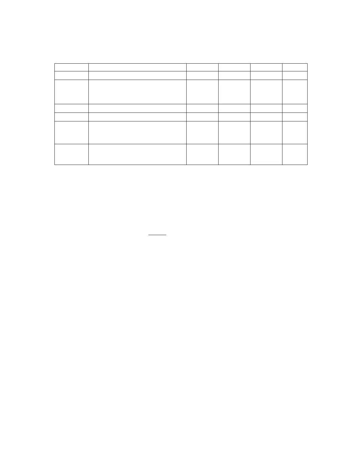
Table A-4a. 20.97 MHz Clock Control Timing
(V
DD
and
V
DDSYN
= 5.0 Vdc ±5%, V
SS
= 0 Vdc, T
A
= T
L
to T
H,
32.768 kHz reference
)
Num Characteristic Symbol Min Max Unit
1 PLL Reference Frequency Range f
ref
25 50 kHz
2 System Frequency
1
dc 20.97
On-Chip PLL System Frequency f
sys
0.131 20.97 MHz
External Clock Operation dc 20.97
3 PLL Lock Time
2,3,4,5
t
lpll
—20ms
4 VCO Frequency
6
f
VCO
— 2 (f
sys
max) MHz
5 Limp Mode Clock Frequency
SYNCR X bit = 0
SYNCR X bit = 1
f
limp
—
—
f
sys
max/2
f
sys
max
MHz
6 CLKOUT Stability
2,3,4,7
Short term (5 µs interval)
Long term (500 µs interval)
C
stab
–0.5
–0.05
0.5
0.05
%
Fr
ees
cale S
em
iconduct
or
, I
Freescale Semiconductor, Inc.
For More Information On This Product,
Go to: www.freescale.com
nc...