MC68332 ELECTRICAL CHARACTERISTICS
USER’S MANUAL A-7
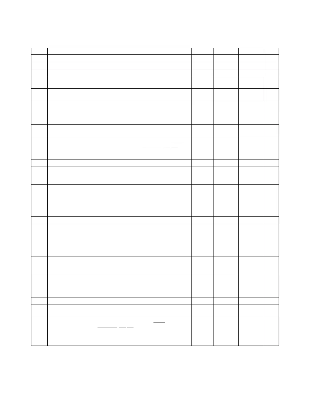
Table A-5a. 20.97 MHz DC Characteristics
(V
DD
and V
DDSYN
= 5.0 Vdc ± 5%, V
SS
= 0 Vdc, T
A
= T
L
to T
H
)
Num Characteristic Symbol Min Max Unit
1 Input High Voltage V
IH
0.7 (V
DD
)V
DD
+ 0.3 V
2 Input Low Voltage V
IL
V
SS
– 0.3 0.2 (V
DD
)V
3 Input Hysteresis
1
V
HYS
0.5 — V
4 Input Leakage Current
2
V
in
= V
DD
or V
SS
Input-only pins
I
in
–2.5 2.5 µA
5 High Impedance (Off-State) Leakage Current
2
V
in
= V
DD
or V
SS
All input/output and output pins
I
OZ
–2.5 2.5
µA
6 CMOS Output High Voltage
2, 3
I
OH
= –10.0 µAGroup 1, 2, 4 input/output and all output pins
V
OH
V
DD
– 0.2 — V
7 CMOS Output Low Voltage
2
I
OL
= 10.0 µAGroup 1, 2, 4 input/output and all output pins
V
OL
— 0.2 V
8 Output High Voltage
2, 3
I
OH
= –0.8 mAGroup 1, 2, 4 input/output and all output pins
V
OH
V
DD
– 0.8 — V
9 Output Low Voltage
2
I
OL
= 1.6 mAGroup 1 I/O Pins, CLKOUT, FREEZE/QUOT, IPIPE
I
OL
= 5.3 mAGroup 2 and Group 4 I/O Pins, CSBOOT, BG/CS
I
OL
= 12 mAGroup 3
V
OL
—
—
—
0.4
0.4
0.4
V
10 Three State Control Input High Voltage V
IHTSC
1.6 (V
DD
) 9.1 V
11 Data Bus Mode Select Pull-up Current
5
V
in
= V
IL
DATA[15:0]
V
in
= V
IH
DATA[15:0]
I
MSP
—
–15
–120
—
µA
12 V
DD
Supply Current
6
RUN
4
RUN, TPU emulation mode
LPSTOP, 32.768 kHz crystal, VCO Off (STSIM = 0)
LPSTOP (External clock input frequency = maximum f
sys
)
I
DD
I
DD
S
IDD
S
IDD
—
—
—
—
140
150
350
5
mA
mA
µA
mA
13 Clock Synthesizer Operating Voltage V
DDSYN
4.75 5.25 V
14 V
DDSYN
Supply Current
6
32.768 kHz crystal, VCO on, maximum f
sys
External Clock, maximum f
sys
LPSTOP, 32.768 kHz crystal, VCO off (STSIM = 0)
32.768 kHz crystal, V
DD
powered down
I
DDSYN
I
DDSYN
S
IDDSYN
I
DDSYN
—
—
—
—
2
6
150
100
mA
mA
µA
µA
15 RAM Standby Voltage
7
Specified V
DD
applied
V
DD
= V
SS
V
SB
0.0
3.0
5.25
5.25
V
16 RAM Standby Current
6,7,10
Normal RAM operationV
DD
> V
SB
– 0.5 V
Transient conditionV
SB
– 0.5 V ≥ V
DD
≥ V
SS
+ 0.5 V
Standby operationV
DD
< V
SS
+ 0.5 V
I
SB
—
—
10
3
50
µA
mA
µA
17 Power Dissipation
8
P
D
— 766 mW
18 Input Capacitance
2, 9
All input-only pins
All input/output pins
C
in
—
—
10
20
pF
19 Load Capacitance
2
Group 1 I/O Pins and CLKOUT, FREEZE/QUOT, IPIPE
Group 2 I/O Pins and CSBOOT, BG/CS
Group 3 I/O pins
Group 4 I/O pins
C
L
—
—
—
—
90
100
130
200
pF
Fr
ees
cale S
em
iconduct
or
, I
Freescale Semiconductor, Inc.
For More Information On This Product,
Go to: www.freescale.com
nc...