MC68332 ELECTRICAL CHARACTERISTICS
USER’S MANUAL A-29
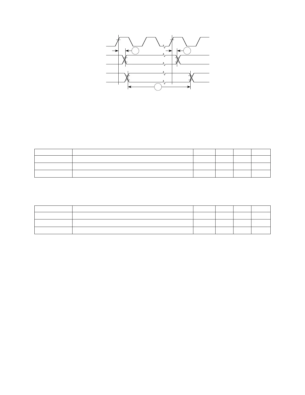
Figure A-20 TPU Timing Diagram
NOTES:
1.AC timing is shown with respect to 20% V
DD
and 70% V
DD
levels.
2.Timing not valid for external T2CLK input.
3.Maximum load capacitance for CLKOUT pin is 90 pF.
4.Maximum load capacitance for TPU output pins is 100 pF.
Table A-10 16.78 MHz Time Processor Unit Timing
(V
DD
and
V
DDSYN
= 5.0 Vdc ±10%, V
SS
= 0 Vdc, T
A
= T
L
to T
H, 32.768 kHz reference
)
Num Rating Symbol Min Max Unit
1 CLKOUT High to TPU Output Channel Valid t
CHTOV
223ns
2 CLKOUT High to TPU Output Channel Hold t
CHTOH
020ns
3 TPU Input Channel Pulse Width t
TIPW
4—t
cyc
Table A-11 20.97 MHz Time Processor Unit Timing
(V
DD
and
V
DDSYN
= 5.0 Vdc ±10%, V
SS
= 0 Vdc, T
A
= T
L
to T
H, 32.768 kHz reference
)
Num Rating Symbol Min Max Unit
1 CLKOUT High to TPU Output Channel Valid t
CHTOV
218ns
2 CLKOUT High to TPU Output Channel Hold t
CHTOH
015ns
3 TPU Input Channel Pulse Width t
TIPW
4—t
cyc
TPU I/O TIM
CLKOUT
TPU OUTPUT
TPU INPUT
21
3
Fr
ees
cale S
em
iconduct
or
, I
Freescale Semiconductor, Inc.
For More Information On This Product,
Go to: www.freescale.com
nc...