P74x/EN SC/N
1, P742, P743 (SC) 13-
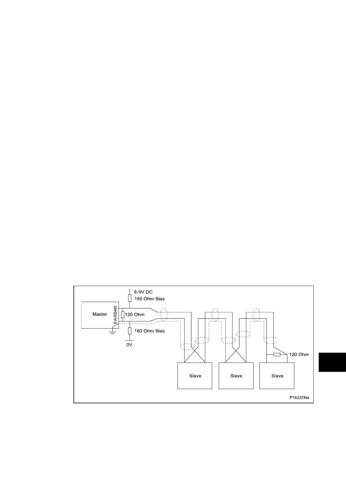
1.2.1.3 Bus connections & topologies
The EIA(RS)485 standard requires that each device be directly connected to the physical
cable that is the communications bus. Stubs and tees are expressly forbidden, as are star
topologies. Loop bus topologies are not part of the EIA(RS)485 standard and are forbidden
by it.
Two-core screened cable is recommended. The specification of the cable will be dependent
on the application, although a multi-strand 0.5mm
2
per core is normally adequate. Total
cable length must not exceed 1000m. The screen must be continuous and connected to
ground at one end, normally at the master connection point; it is important to avoid
circulating currents, especially when the cable runs between buildings, for both safety and
noise reasons.
This product does not provide a signal ground connection. If a signal ground connection is
present in the bus cable then it must be ignored, although it must have continuity for the
benefit of other devices connected to the bus. At no stage must the signal ground be
connected to the cables screen or to the product’s chassis. This is for both safety and noise
reasons.
1.2.1.4 Biasing
It may also be necessary to bias the signal wires to prevent jabber. Jabber occurs when the
signal level has an indeterminate state because the bus is not being actively driven. This
can occur when all the slaves are in receive mode and the master is slow to turn from
receive mode to transmit mode. This may be because the master purposefully waits in
receive mode, or even in a high impedance state, until it has something to transmit. Jabber
causes the receiving device(s) to miss the first bits of the first character in the packet, which
results in the slave rejecting the message and consequentially not responding. Symptoms of
this are poor response times (due to retries), increasing message error counters, erratic
communications, and even a complete failure to communicate.
Biasing requires that the signal lines be weakly pulled to a defined voltage level of about 1V.
There should only be one bias point on the bus, which is best situated at the master
connection point. The DC source used for the bias must be clean; otherwise noise will be
injected. Note that some devices may (optionally) be able to provide the bus bias, in which
case external components will not be required.
FIGURE 1: EIA(RS)485 BUS CONNECTION ARRANGEMENTS
It is possible to use the products field voltage output (48V DC) to bias the bus using values
of 2.2kΩ (½W) as bias resistors instead of the 180Ω resistors shown in the above diagram.