P/N 960-000180R_Rev. 1 {EDP #233427} © 2016, JAPAN CASH MACHINE CO., LTD.
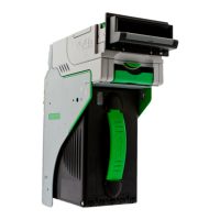
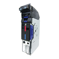
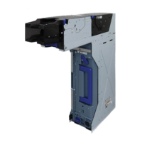
Installation DBV® Series DBV-400 Banknote Validator Section 2
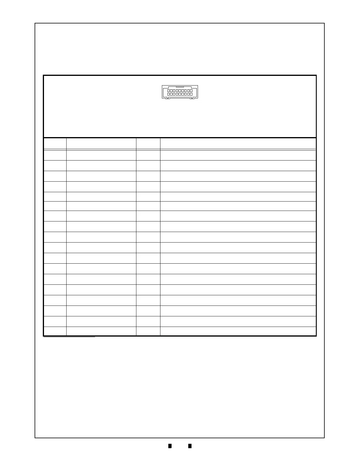
Connector Pin Assignments
Table 2-4 through Table 2-11 list the DBV-400 Unit’s pin assignments.
MDB/Photo-Coupler Isolation Connector Pin Assignments
Table 2-4 lists the DBV-400 ID-003 MDB/Photo-Coupler Isolation Connector Pin Assignments.
Table 2-4 DBV-400 ID-003 MDB/Photo-Coupler Isolation Connector Pin Assignments
CN1 Connector (DBV-400 Side): 74164-0118 (Molex)
Housing (Cable Side): 50-57-9309 SL
™
Crimp Housing, Single Row, Version D, Back Ribs, 9 Circuits (Molex)
015-04-5184 2.54mm SL
™
Interim Clip, 18 Circuits, Polarized (Molex)
16-02-0069 SL
™
Crimp Terminal, Series70058, Female, with Tin (Sn) Plated Contact, 24-30 AWG
(Maximum Insulation Diameter: Less than φ1.52) (Molex)
Recommended Wire (for Power Supply and Power Ground): Insulation Diameter AWG #24 (Maximum Insulation Diameter: Less than φ1.52)
Recommended Wire (for Signal Ground): AWG #24 - 30 (Maximum Insulation Diameter: Less than φ1.52)
Pin No. Signal Name
I/O
*
*. I/O (input/output) is the terminal as viewed from the Banknote Validator’s side.
Function
1 +12V - +24V - Power Supply
2GND
-
Power Ground (0V DC)
3 +12V - +24V
-
Power Supply
4GND
-
Power Ground (0V DC)
5TXD
OUT
Serial Communication Output Signal Line
6RXD
IN
Serial Communication Input Signal Line
7COMMON
-
Photo-Coupler Common Signal Line
8
--
Reserved
9
--
Reserved
10 GND
-
Signal Ground (0V DC)
11
--
Reserved
12
--
Reserved
13
--
Reserved
14
--
Reserved
15
--
Reserved
16
--
Reserved
17
--
Reserved
18 VCCSYNC IN Wakeup Input Signal Line