P/N 960-000180R_Rev. 1 {EDP #233427} © 2016, JAPAN CASH MACHINE CO., LTD.
DBV® Series
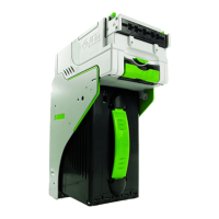
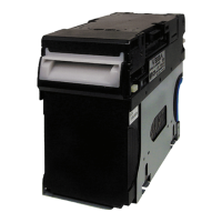
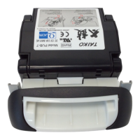
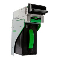
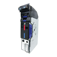
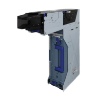
DBV-400 Banknote Validator
Section 5
This chapter provides for the DBV
®
Series DBV-
400 Banknote Validator Unit Wiring Diagrams for
the following items:
• System Wiring Diagram
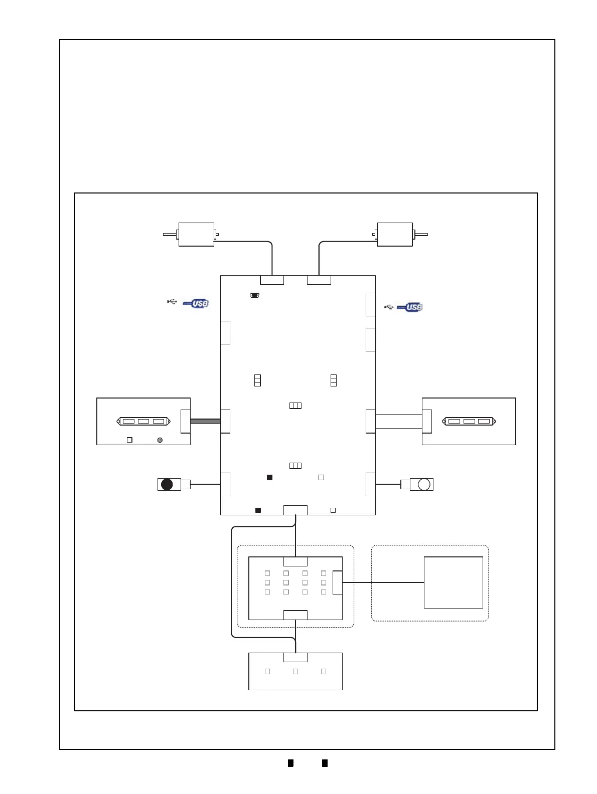
Figure 5-1 DBV-400 System Wiring Diagram
System Wiring Diagram
Figure 5-1 DBV-400 System Wiring Diagram
PT2
CPU Board
Inside Validation Sensor Board
CN7
18-Pin FFC
Transport Motor EncoderStacker Motor Encoder
Pusher Home Sensor
Box In Sensor
CN5
CN9
CN1
CN1
Host Interface and Power Input
Molex C-Grid 18
For the Debugging Tool
CN8
CN10 CN2
CN11
Program Download
Side Sensor
Entrance Sensor
Entrance Sensor
Exit Sensor
Exit Sensor
CN6
CN4 CN3
Transport MotorStacker Motor
Host Interface
PI4 PI3
PI1
Outside Validation Sensor Board
CN1
Error Lamp
Operation Button
PI1
PT2
Full Color
Bezel LED Board
CN1
Full Color
Optional Bezel LED Board
CN1
CN3
NFC Module
CN2
OptionOption
Validation Sensor Module
Validation Sensor Module
LED2
LED1PT1
(Light-Receiving)
Side Sensor
3-Color LED
(LED)
(Transport)
(Emission)
(LED)
(Transport)