MS51
Nov. 28, 2019 Page 6 of 491 Rev 1.00
MS51 32K SERIES TECHNICAL REFERENCE MANUAL
LIST OF FIGURES
Figure 4.1-1 Pin Assignment of LQFP-32 Package ....................................................................... 17
Figure 4.1-2 Pin Assignment of LQFP-32 Package ....................................................................... 18
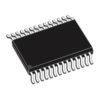
Figure 4.1-3 Pin Assignment of TSSOP28 Package ..................................................................... 19
Figure 4.1-4 Pin Assignment of TSSOP20 Package ..................................................................... 19
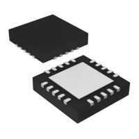
Figure 4.1-5 Pin Assignment of QFN20 Package .......................................................................... 20
Figure 5.1-1 Functional Block Diagram .......................................................................................... 25
Figure 6.1-1 MS51 Program Memory Map .................................................................................... 27
Figure 6.1-2 SPROM Memory Mapping And SPROM Security Mode ........................................... 28
Figure 6.1-3. CONFIG0 Any Reset Reloading ............................................................................... 29
Figure 6.1-4. CONFIG2 Power-On Reset Reloading ..................................................................... 31
Figure 6.1-5 Data Memory Map ..................................................................................................... 34
Figure 6.1-6 Internal 256 Bytes RAM Addressing .......................................................................... 35
Figure 6.2-1 Clock System Block Diagram .................................................................................. 201
Figure 6.2-2 Brown-out Detection Block Diagram ........................................................................ 214
Figure 6.2-3 Boot Selecting Diagram ........................................................................................... 224
Figure 6.3-1 CONFIG0 Any Reset Reloading .............................................................................. 268
Figure 6.3-2 CONFIG2 Power-On Reset Reloading .................................................................... 270
Figure 6.4-1 Quasi-Bidirectional Mode Structure ......................................................................... 273
Figure 6.4-2 Push-Pull Mode Structure ........................................................................................ 273
Figure 6.4-3 Input-Only Mode Structure ...................................................................................... 274
Figure 6.4-4 Open-Drain Mode Structure .................................................................................... 274
Figure 6.4-5 Pin Interface Block Diagram .................................................................................... 275
Figure 6.5-1 Timer/Counters 0 and 1 in Mode 0 .......................................................................... 288
Figure 6.5-2 Timer/Counters 0 and 1 in Mode 1 .......................................................................... 288
Figure 6.5-3 Timer/Counters 0 and 1 in Mode 2 .......................................................................... 288
Figure 6.5-4 Timer/Counter 0 in Mode 3 ...................................................................................... 289
Figure 6.5-5 Timer 2 Block Diagram ............................................................................................ 297
Figure 6.5-6 Timer 2 Auto-Reload Mode and Input Capture Module Functional Block Diagram 298
Figure 6.5-7 Timer 2 Compare Mode and Input Capture Module Functional Block Diagram...... 299
Figure 6.5-8 Timer 3 Block Diagram ............................................................................................ 314
Figure 6.6-1 PWM0 Block Diagram .............................................................................................. 320
Figure 6.6-2 PWM1/2/3 Block Diagram........................................................................................ 321
Figure 6.6-3 PWM0 and Fault Brake Output Control Block Diagram .......................................... 322
Figure 6.6-4 PWM1/2/3 Control Block Diagram ........................................................................... 323
Figure 6.6-5 PWM Edge-aligned Type Waveform ....................................................................... 324
Figure 6.6-6 PWM Center-aligned Type Waveform ..................................................................... 324