V
IL
V
IN
V
DD
V
IH
V
INTERNAL
V
HYS
(SIUL register)
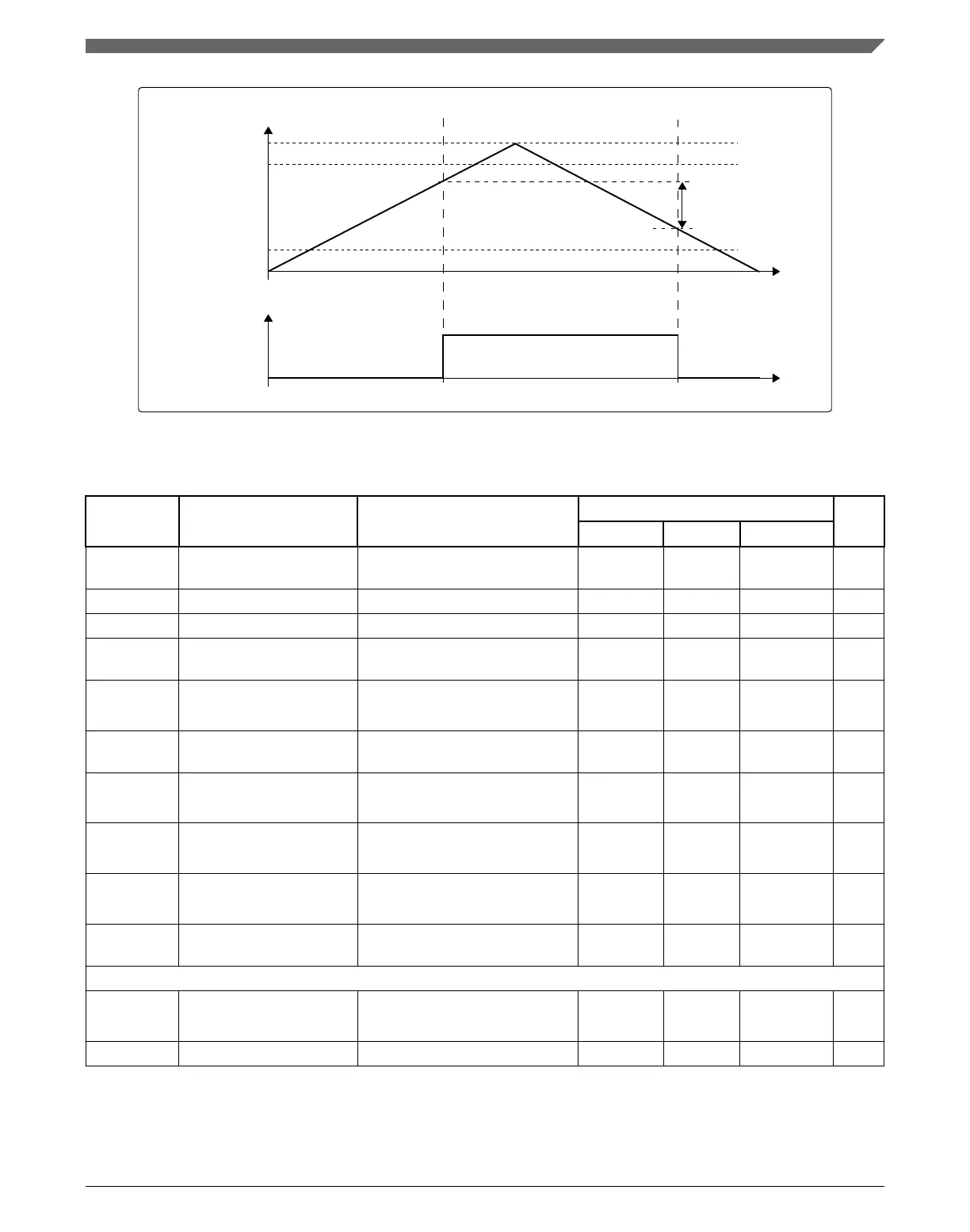
Figure 3. I/O input DC electrical characteristics definition
Table 7. I/O input DC electrical characteristics
Symbol Parameter
1
Conditions Value
2
Unit
Min Typ Max
VIHTTL TTL input high level 3.0 V < V
DD_HV_IO
< 5.5 V 2.0 — V
DD_HV_IO
+
0.3
V
VILTTL TTL input low level 3.0 V < V
DD_HV_IO
< 5.5 V V
SS
-0.3 — 0.6 V
VHYSTTL TTL level input hysteresis 3.0 V < V
DD_HV_IO
< 5.5 V 0.3 — — V
VDRFTTTL TTL Input VIL/VIH
temperature drift
— — — 100
3
mV
VIHCMOS_H CMOS input high level
(with hysteresis)
3.0 V < V
DD_HV_IO
< 5.5 V 0.65 *
V
DD_HV_IO
— V
DD_HV_IO
+ 0.3
V
VIHCMOS CMOS input high level
(without hysteresis)
3.0 V < V
DD_HV_IO
< 5.5 V 0.55 *
V
DD_HV_IO
— V
DD_HV_IO
+
0.3
V
VILCMOS_H CMOS input low level (with
hysteresis)
3.0 V < V
DD_HV_IO
< 5.5 V V
SS
-0.3 — 0.35 *
V
DD_HV_IO
V
VILCMOS CMOS input low level
(without hysteresis)
3.0 V < V
DD_HV_IO
< 5.5 V V
SS
-0.3 — 0.4 *
V
DD_HV_IO
V
VHYSCMOS CMOS input hysteresis 3.0 V < V
DD_HV_IO
< 5.5 V 0.1 *
V
DD_HV_IO
— — V
VDRFTCMO
S
CMOS Input VIL/VIH
temperature drift
— — — 100
3
mV
INPUT CHARACTERISTICS
4
I
LKG
Digital input leakage GPIO pins
V
SS
< V
IN
< V
DD_HV_IO
-1.0 — 1.0 µA
C
IN
Input capacitance GPIO and Input pins — — 8 pF
1. Supported input levels vary according to pad types. Pad type "pad_sr_hv" supports only the CMOS input level, while pad
type "pad_isatww_st_hv" supports TTL and CMOS levels. Refer to the IO spreadsheet attached to the Reference Manual
for the pad type of each pin.
I/O pad specification
SPC5746R Microcontroller Data Sheet, Rev. 6, 06/2017
NXP Semiconductors 13

 Loading...


