2. TTL level input specifications apply to the digital inputs on the analog input pins, and not the GPIO pins on the device.
3. In a 1 ms period, assuming stable voltage and a temperature variation of ±30 °C, VIL/VIH shift is within ±50 mV. For
SENT requirement, refer to Note in the "I/O pad current specifications" section.
4. For LFAST, microsecond bus, and LVDS input characteristics, refer to dedicated communication module chapters.
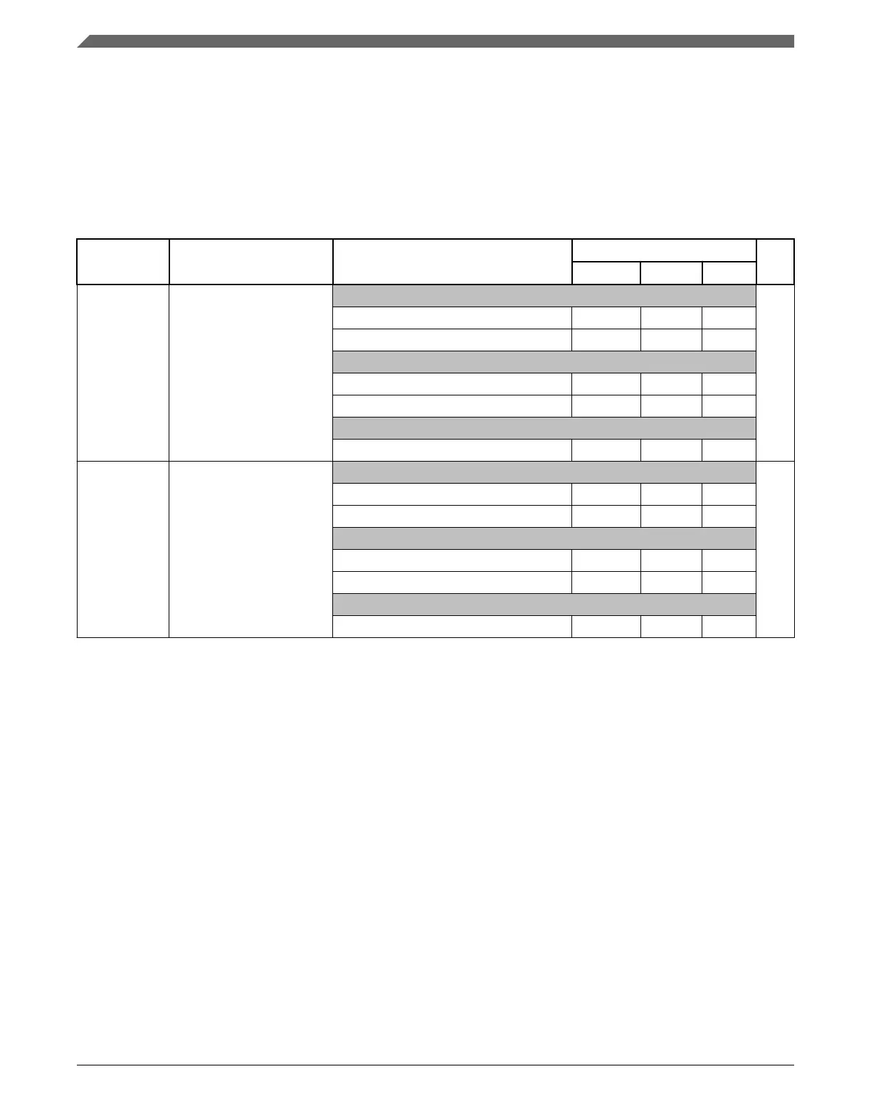
The following table provides the current specifications for the GPIO pad weak pull-up
and pull-down.
Table 8. GPIO Pull-Up/Down DC electrical characteristics
Symbol Parameter Conditions Value Unit
Min Typ Max
|IWPU| Weak pull-up current
absolute value
1
Vin = VIH = 0.65 * V
DD_HV_IO
µA
4.5V < V
DD_HV_IO
< 5.5V 30 — —
3.0V < V
DD_HV_IO
< 3.6V 18 — —
Vin = VIL = 0.35 * V
DD_HV_IO
4.5V < V
DD_HV_IO
< 5.5V — — 120
3.0V < V
DD_HV_IO
< 3.6V — — 80
Vin = VIL = 1.1V (TTL)
4.5V < V
DD_HV_IO
< 5.5V — — 130
|IWPD| Weak pull-down current
absolute value
Vin = VIH = 0.65 * V
DD_HV_IO
µA
4.5V < V
DD_HV_IO
< 5.5V — — 120
3.0V < V
DD_HV_IO
< 3.6V — — 80
Vin = VIL = 0.35 * V
DD_HV_IO
4.5V < V
DD_HV_IO
< 5.5V 30 — —
3.0V < V
DD_HV_IO
< 3.6V 18 — —
Vin = VIL = 0.9V (TTL)
4.5V < V
DD_HV_IO
< 5.5V 16 — —
1. Weak pull-up/down is enabled within tWK_PU = 1 µs after internal/external reset has been asserted. Output voltage will
depend on the amount of capacitance connected to the pin.
I/O pad specification
SPC5746R Microcontroller Data Sheet, Rev. 6, 06/2017
14 NXP Semiconductors

 Loading...


