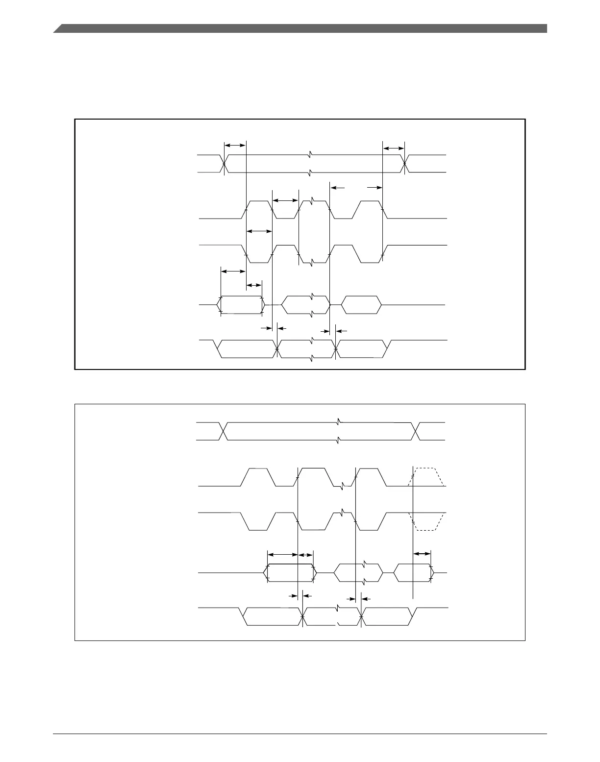
9. P is the number of clock cycles added to delay the DSPI input sample point and is software programmable using
DSPI_MCR[SMPL_PT]. The value must be 0, 1 or 2. If the baud rate divide ratio is /2 or /3, this value is automatically set
to 1.
10. SOUT Data Valid and Data hold are independent of load capacitance if SCK and SOUT load capacitances are the same
value.
Data
Data
Last Data
First Data
First Data
Last Data
SIN
SOUT
SCK Output
SCK Output
(CPOL = 0)
PCSx
(CPOL = 1)
t
SCK
t
SDC
t
SDC
CSC
t
t
ASC
t
t
SUI
HI
t
SUO
t
HO
Figure 33. DSPI CMOS master mode – modified timing, CPHA = 0
SIN
PCSx
SCK Output
SCK Output
SOUT
First Data
First Data
(CPOL=1)
(CPOL=0)
Last Data
Last Data
DataData
Data
t
SUI
t
HI
t
SUO
t
HO
t
HI
Figure 34. DSPI CMOS master mode – modified timing, CPHA = 1
AC specifications
SPC5746R Microcontroller Data Sheet, Rev. 6, 06/2017
72 NXP Semiconductors

 Loading...


