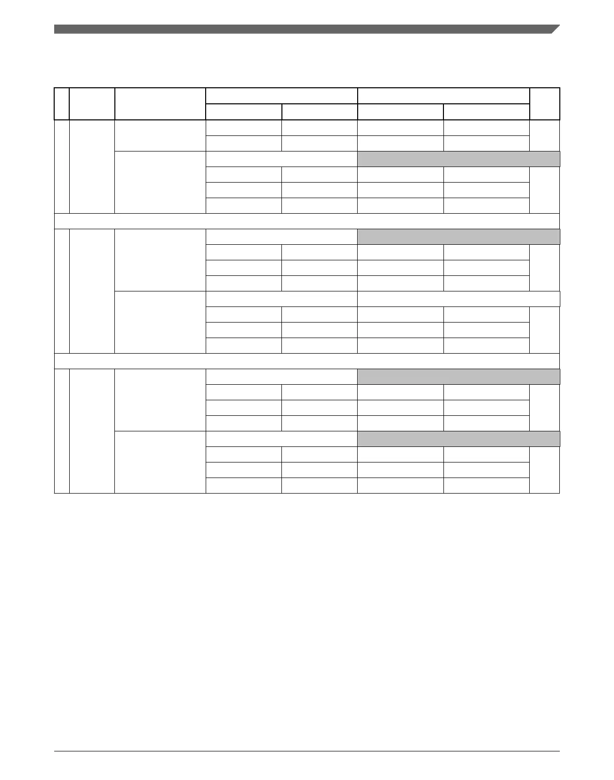
Table 41. DSPI CMOS master modified timing (full duplex and output only) - MTFE = 1,
CPHA = 0 or 1 (continued)
# Symbol Characteristic Condition Value
1
Unit
Pad drive
2
Load (C
L
) Min Max
CPHA = 0
9
Strong 0 pF -1 + (P
8
x t
SYS
, 3
) —
Medium 0 pF -1 + (P
8
x t
SYS
, 3
) —
SIN hold time from
SCK CPHA = 1
9
SCK drive strength
Very strong 0 pF -1.0 — ns
Strong 0 pF -1.0 —
Medium 0 pF -1.0 —
SOUT data valid time (after SCK edge)
9 t
SUO
SOUT data valid time
from SCK
CPHA = 0
9
SOUT and SCK drive strength
Very strong 25 pF — 7.0 + t
SYS
4
ns
Strong 50 pF — 8.0 + t
SYS
4
Medium 50 pF — 16.0 + t
SYS
4
SOUT data valid time
from SCK
CPHA = 1
9
SOUT and SCK drive strength
Very strong 25 pF — 7.0 ns
Strong 50 pF — 8.0
Medium 50 pF — 16.0
SOUT data hold time (after SCK edge)
10 t
HO
SOUT data hold time
after SCK
CPHA = 0
10
SOUT and SCK drive strength
Very strong 25 pF -7.7 + t
SYS
4
— ns
Strong 50 pF -11.0 + t
SYS
4
—
Medium 50 pF -15.0 + t
SYS
4
—
SOUT data hold time
after SCK
CPHA = 1
10
SOUT and SCK drive strength
Very strong 25 pF -7.7 — ns
Strong 50 pF -11.0 —
Medium 50 pF -15.0 —
1. All timing values for output signals in this table are measured to 50% of the output voltage.
2. Timing is guaranteed to same drive capabilities for all signals, mixing of pad drives may reduce operating speeds and may
cause incorrect operation.
3. N is the number of clock cycles added to time between PCS assertion and SCK assertion and is software programmable
using DSPI_CTARx[PSSCK] and DSPI_CTARx[CSSCK]. The minimum value is 2 cycles unless TSB mode or Continuous
SCK clock mode is selected, in which case, N is automatically set to 0 clock cycles (PCS and SCK are driven by the same
edge of DSPI_CLKn).
4. t
SYS
is the period of DSPI_CLKn clock, the input clock to the DSPI module. Maximum frequency is 100 MHz (min t
SYS
= 10
ns).
5. M is the number of clock cycles added to time between SCK negation and PCS negation and is software programmable
using DSPI_CTARx[PASC] and DSPI_CTARx[ASC]. The minimum value is 2 cycles unless TSB mode or Continuous SCK
clock mode is selected, in which case, M is automatically set to 0 clock cycles (PCS and SCK are driven by the same edge
of DSPI_CLKn).
6. t
SDC
is only valid for even divide ratios. For odd divide ratios the fundamental duty cycle is not 50:50. For these odd divide
ratios cases, the absolute spec number is applied as jitter/uncertainty to the nominal high time and low time.
7. PCSx and PCSS using same pad configuration.
8. Input timing assumes an input slew rate of 1 ns (10% - 90%) and uses TTL voltage thresholds.
AC specifications
SPC5746R Microcontroller Data Sheet, Rev. 6, 06/2017
NXP Semiconductors 71

 Loading...


