PG-FP5 CHAPTER 11 SPECIFICATIONS OF TARGET INTERFACE CIRCUITS
R20UT0008EJ0400 Rev. 4.00 Page 198 of 240
Jul 15, 2010
11.3 CLK
It is recommended to supply the target device operating clock from the target system. When supplying the target
device operating clock from the FP5, communication may not be performed normally due to the waveform distortion
caused by wiring of clock lines on the target system. In such a case, add elements such as CMOS buffers to the target
system as necessary so as to adjust the waveform.
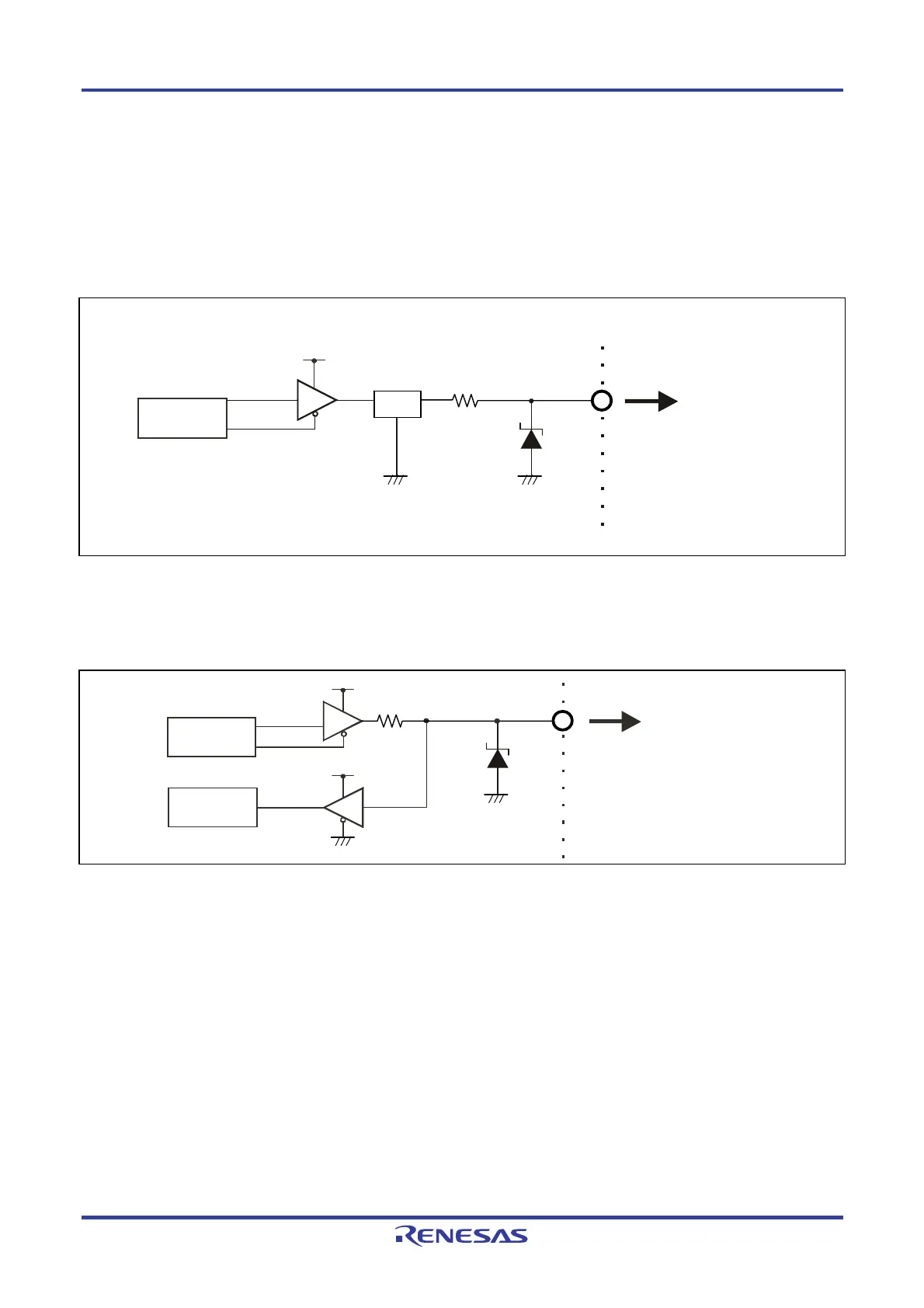
Figure 11-3. CLK Pins
11.4 FLMD0 and FLMD1
Figure 11-4. FLMD0 and FLMD1 Pins
Noise filter
NFL21SP506
33Ω
FP5
EMZ6.8 E
Signal output
Circuit
74LV125
Signal
Target System
FP5
Target System
Signal
EMZ6.8 E
Signal output
circuit
Self-testing
circuit
74LV125
74LV125
FP5_VDD
FP5_VDD
33 Ω
FP5_V
DD
or
FP5_VDD2