PG-FP5 APPENDIX D ELECTRICAL SPECIFICATIONS OF REMOTE INTERFACE
R20UT0008EJ0400 Rev. 4.00 Page 228 of 240
Jul 15, 2010
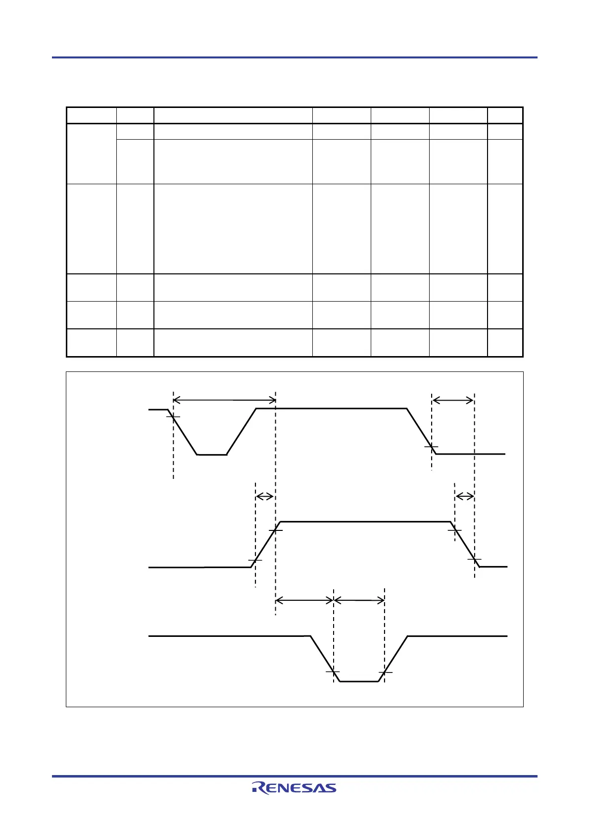
D.3.2 Bank mode
(1/2)
Pin name Symbol Parameter or Conditions MIN. TYP. MAX. Unit
tPLH Rise time (IO = 8 mA) 5 ns CONN
BUSY
PASS
ERROR
t
PHL Fall time (IO = 8 mA) 5 ns
BANK0
BANK1
BANK2
VRF
START
CLEAR
t
PLIN Low-level width of input signal 50 ms
tPPOCN
Time from turning on the power of the FP5
until the rise of the CONN signal
8 s
tPCNPO
Time from turning off the power of the FP5
until the fall of the CONN signal
1 s
tPCNIN
Time from the rise of the CONN signal until
the input signal is acknowledged
1 ms
FP5_POWER
button
CONN
t
PLIN
t
PHL
t
PLH
t
PCNPO
t
PCNIN
BANK0
BANK1
BANK2
START
VRF
CLEAR
t
PPOCN