PG-FP5 CHAPTER 10 NOTES ON TARGET SYSTEM DESIGN
R20UT0008EJ0400 Rev. 4.00 Page 191 of 240
Jul 15, 2010
CHAPTER 10 NOTES ON TARGET SYSTEM DESIGN
This chapter explains the basic notes on the target system for writing to the flash memory in the target device, using the
FP5.
(1/3)
Target Device Pin Recommended Design
Common item
• When connecting the FP5 output signal pins, refer to CHAPTER 11 SPECIFICATIONS OF TARGET
INTERFACE CIRCUITS and pull up (or pull down) with a resistance in compliance with the device
specifications (V
IH, VIL).
• When connecting the FP5 input signal pins, refer to CHAPTER 11 SPECIFICATIONS OF TARGET
INTERFACE CIRCUITS and pull up (or pull down) with a resistance in compliance with the device
specifications (I
OH, IOL).
• After turning on the FP5 power supply, the states of the various terminals before and after command
execution will be as follows:
-The RESET
¯¯¯¯¯¯
pin will use Low output. (However, it will be Hi-Z if Hi-Z is set with the FP5 Manager.)
-The pins other than the RESET
¯¯¯¯¯¯
pin and GND pin will be in the Hi-Z state.
• Observe the waveforms of the terminals on the target device. If the electrical specifications are not
satisfactory, then shape the waveforms by adding buffers, and so on. If using a cable other than the
included target cable, be sure to check the waveforms.
• Basically, the power supply and clock for the target device should be supplied from the target system.
This, however, excludes some target devices which require supply from the FP5. When outputting the
clock from the FP5, if the input specs of the target device are not satisfactory, then be sure to shape
the waveform.
• Be sure to consider contact quality (such as conductivity, durability) of the connector connected to the
target cable. We recommend a mechanism that connects to the GND pin.
When the FP5 RESET
¯¯¯¯¯¯
pin is in the output mode (when the [Enable target RESET] of the [Command
options] are not checked), do not connect the RESET
¯¯¯¯¯¯
signal generating circuit of the target system to the
FP5 RESET
¯¯¯¯¯¯
signal, or signal collision would occur.
Do not connect the RESET
¯¯¯¯¯¯
signal generator on the target system to the RESET
¯¯¯¯¯¯
signal of the FP5.
Otherwise, a signal conflict will occur. To avoid a conflict, isolate the RESET
¯¯¯¯¯¯
signal generator from the
RESET
¯¯¯¯¯¯
signal of the FP5. Do not generate RESET
¯¯¯¯¯¯
while the FP5 is connected. This must be especially
noted in a target system in which an external watchdog timer is used.
RESET
¯¯¯¯¯¯
Connect the RESET
¯¯¯¯¯¯
signal of the FP5 at a point where the status of the FP5 RESET
¯¯¯¯¯¯
signal and that of the
CPU RESET
¯¯¯¯¯¯
pin are the same.
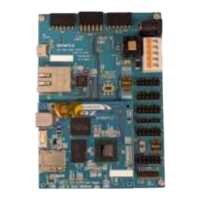
Correct connection <1>:
Target device
FP5 RESET
RESET
RESET IC
RESET IC is an open-drain type circuit. Connect a resistor to the portion above enclosed in the dotted
line, as necessary.