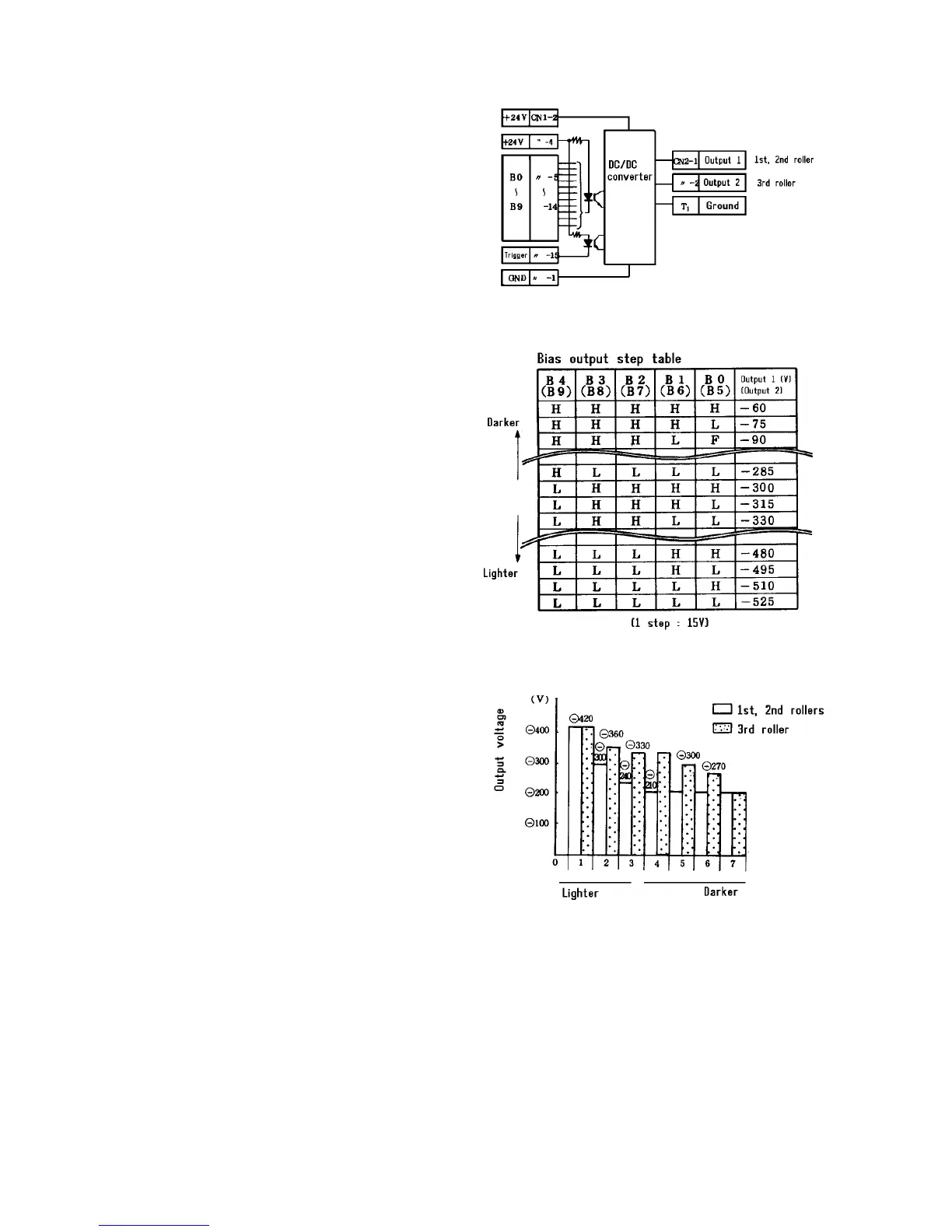
2.9.12 Development bias control
The development bias is output from a voltage regulated
power pack. It is controlled by turning 10
phototransistors ON and OFF with control signals
B0-B9, and the output is within the range -60 to -525V.
The control signals B0-B4 are sent to output 1 (1st and
2nd development rollers), and control signals B5-B9 are
sent to output 2 (3rd development roller).
The bias voltage is controlled by the selected image
density level (including the AID mode) and
compensation by the process control.
Bias control by image density level
The bias voltages applied to the 1st, 2nd, and 3rd rollers
change with the image density level selected by the
image density keys as shown in the figure.