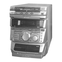
MAP-S1
MAP-S1
4343
For Schematic Diagrams.
Note:
• All capacitors are in μF unless otherwise noted. (p: pF) 50
WV or less are not indicated except for electrolytics and
tantalums.
• All resistors are in Ω and 1/4 W or less unless otherwise
specifi ed.
• 2 : Nonfl ammable resistor.
• C : Panel designation.
THIS NOTE IS COMMON FOR PRINTED WIRING BOARDS AND SCHEMATIC DIAGRAMS.
(In addition to this, the necessary note is printed in each block.)
• A : B+ Line.
• B : B– Line.
• Voltages and waveforms are dc with respect to ground
under no-signal (detuned) conditions.
no mark
: TUNER (FM)
( ) : CD
< > : TUNER (DAB)
[ ] : USB
*
: Impossible to measure
• Voltages are taken with VOM (Input impedance 10 M).
Voltage variations may be noted due to normal production
tolerances.
• Waveforms are taken with a oscilloscope.
Voltage variations may be noted due to normal production
tolerances.
• Circled numbers refer to waveforms.
• Signal path.
F : AUDIO
f : TUNER
J : CD PLAY
E : USB
a : Bluetooth
d : LAN
G : WIRELESS LAN
• Abbreviation
CND : Canadian model
HK : Hong Kong model
MY : Malaysia model
For Printed Wiring Boards.
Note:
• X : Parts extracted from the component side.
• Y : Parts extracted from the conductor side.
• : Pattern from the side which enables seeing.
(The other layers’ patterns are not indicated.)
• Circuit Boards Location
• Indication of transistor.
C
B
These are omitted.
E
Q
Caution:
Pattern face side:
(Conductor Side)
Parts face side:
(Component Side)
Parts on the pattern face side seen
from the pattern face are indicated.
Parts on the parts face side seen from
the parts face are indicated.
• Abbreviation
CND : Canadian model
HK : Hong Kong model
MY : Malaysia model
Caution:
Pattern face side:
(SIDE B)
Parts face side:
(SIDE A)
Parts on the pattern face side seen
from the pattern face are indicated.
Parts on the parts face side seen from
the parts face are indicated.
Note:
The components identi-
fi ed by mark 0 or dotted
line with mark 0 are criti-
cal for safety.
Replace only with part
number specifi ed.
Note:
Les composants identifi és
par une marque 0 sont
critiques pour la sécurité.
Ne les remplacer que par
une pièce portant le nu-
méro spécifi é.
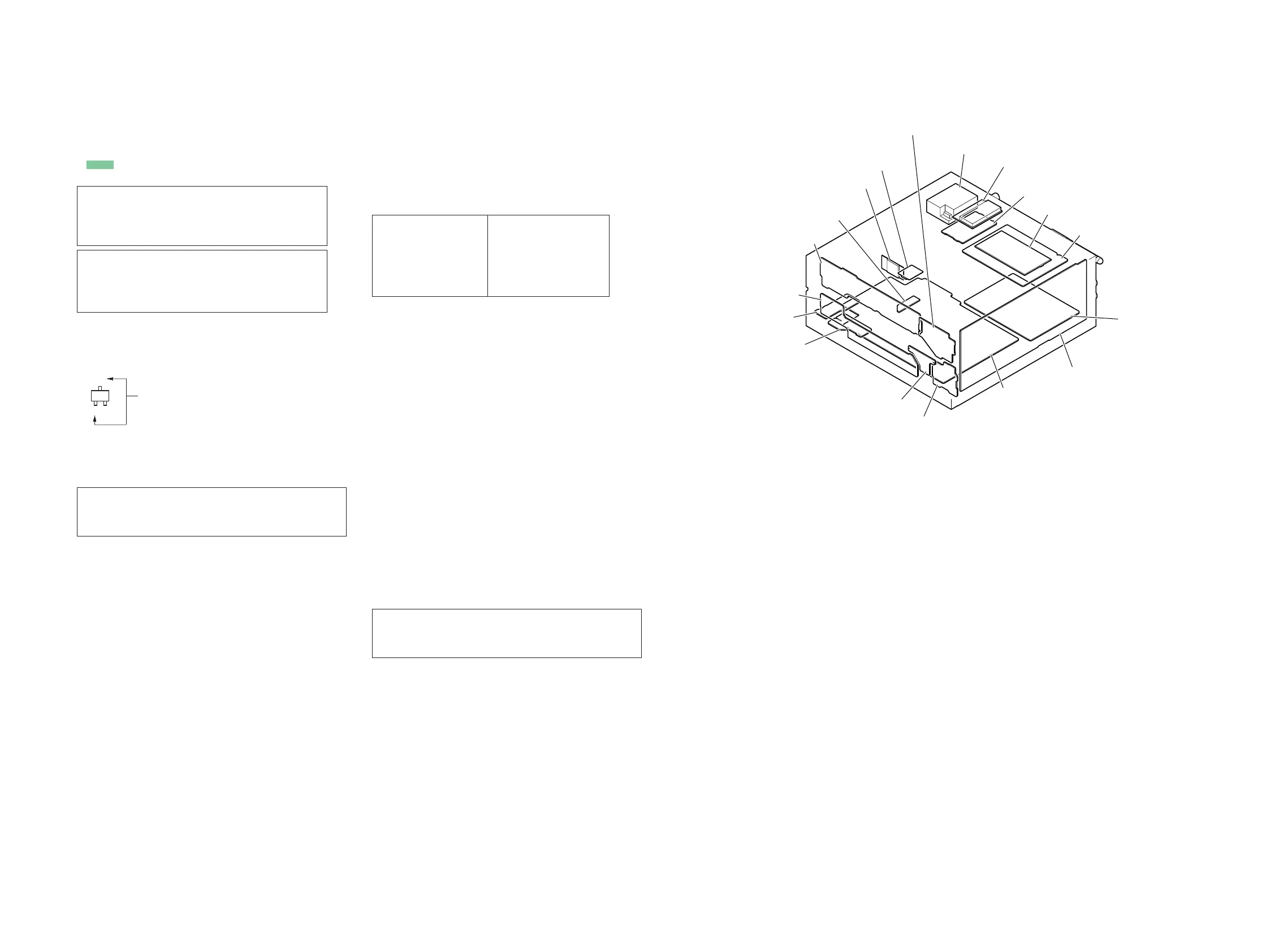
NFC module
(RC-S801) (NFC1)
USB board
FRONT-R board
FRONT-EJECT board
FRONT-KEY board
HP board
MS-091 board
Bluetooth module
(BT1)
FRONT-L board
FRONT board
SUBPOWER boar
MAIN board
TUNER board
AMP board
DAB board
module (DAB tuner) (DAB1)
WiFi module (WIFI1)
NETWORK board
Note: Refer to the “NEW/FORMER DISCRIMINATION OF MAIN,
NETWORK, FRONT-L AND AMP BOARDS” on page 4 for
how to distinguish suffi x-11 and suffi x-12 of MAIN, NET-
WORK, FRONT-L and AMP boards for Canadian model.
Note: Refer to the “NEW/FORMER DISCRIMINATION OF MAIN,
NETWORK, FRONT-L AND AMP BOARDS” on page 4 for
how to distinguish suffi x-11 and suffi x-12 of MAIN, NET-
WORK, FRONT-L and AMP boards for Canadian model.
• MAIN board is multi-layer printed board. However, the
patterns of intermediate layers have not been included in
diagrams.