2-6 (E)
UP-D898MD/X898MD
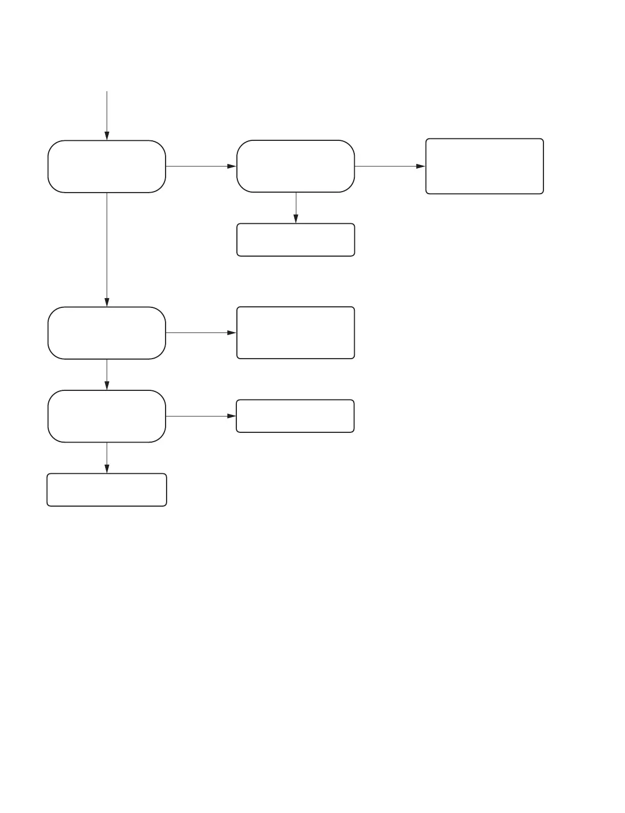
No
Yes
Yes
No
Is the voltage of 26 V to 33 V
output from pins 1 and 2 (VH) of
CN101 on the MA-195 board
during the printing operation?
Is the voltage of 2.0 V to 3.3 V
output from pin 3 (VCONT) of
CN101 on the MA-195 board
during the printing operation?
Replace the switching regulator.
(Refer to Section 3-5.)
FFC: Flexible flat cable
Check the harness connecting
CN101 on the MA-195 board and
CN702 on the switching regulator.
If the symptom persists, replace
the MA-195 board.
(Refer to Section 3-1.)
From the previous page
No
Yes
No
Yes
Is FFC connecting CN701 on the
MA-195 board and the thermal
head normal?
Check the connection of FFC.
If the symptom persists, replace
FFC. (Refer to Section 5.)
Are there any streaks in the paper
feed direction?
Replace the MA-195 board.
(Refer to Section 3-1.)
Replace the thermal head.
(Refer to Section 3-7.)