KCU116 Board User Guide 10
UG1239 (v1.2) September 28, 2018 www.xilinx.com
Chapter2: Board Setup and Configuration
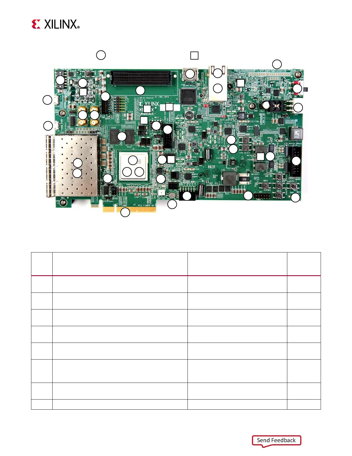
X-Ref Target - Figure 2-1
Figure2‐1: KCU116 Evaluation Board Components
18
5
27
10 9
36
37
34
14
15
6
12
20
21
25
7
13
38
28
29
23
32
31
30
22
4
17
16
26
24
33
33
19
35
3
3
8
11
1
2
00
Round callout references a component
on the front side of the board
Square callout references a component
on the back side of the board
00
5
X18418-041717
Table2‐1: KCU116 Board Component Descriptions
Callout Feature Notes
Schematic
Page
Number
1
Kintex UltraScale+ XCKU5P-2FFVB676E Device,
(with fan-sink on soldered FPGA)
XCKU5P-2FFVB676E
Radian XLX041A
2
DDR4 Component Memory, 1 GB (2x512 MB)
(U150, U153)
Micron MT40A256M16GE-075E 18-19
3 Dual Quad SPI Flash Memory (2x256 Mb) (U2-U3)
Micron MT25QU01GBBB8ESF-0SIT
U2 on top, U3 on bottom of board
4, 6
4 Micro-SD Card Interface, connector (J177)
Molex 5025700893 on bottom of
board
35
5
USB JTAG Interface (U21), with micro-B connector
(J2)
Digilent USB JTAG module
Hirose ZX62D_AB_5P8
17
6
Clock Generation, multi-output clock generator,
SYSCLK and other clocks, 1.8V LVDS (U170)
SI5335A-B02436-GM, four outputs:
300 MHz, 125 MHz, 90 MHz,
33.33 MHz
36
7
Programmable MGT User Clock,
I
2
C programmable user clock 3.3V LVDS (U56)
Silicon Labs SI570BAB0000544DG
(default 156.250 MHz)
37
8 Jitter Attenuated Clock, (U20) Silicon Labs SI5328C-C-GM 28