KCU116 Board User Guide 29
UG1239 (v1.2) September 28, 2018 www.xilinx.com
Chapter3: Board Component Descriptions
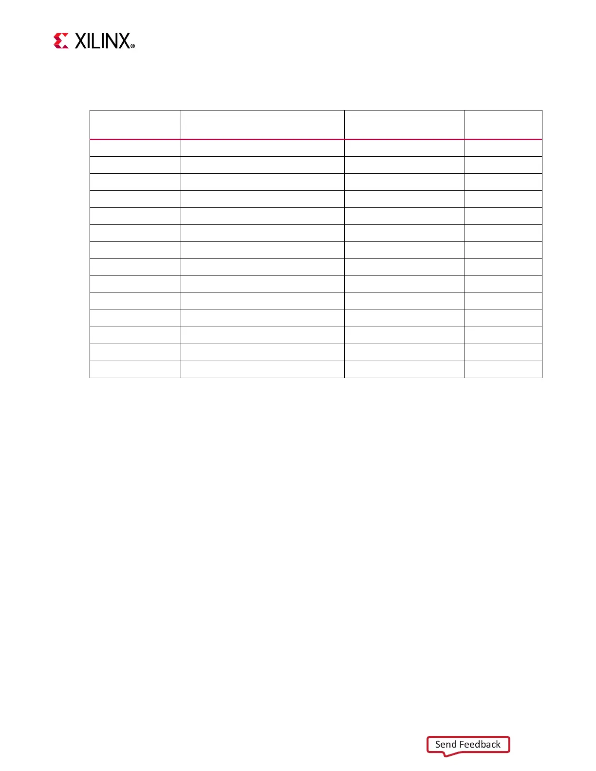
Table 3-6 lists the FPGA connections for each clock.
System Clock
[Figure 2-1, callout 6]
The system clock source is a Silicon Labs SI5335A quad clock generator/buffer (U170). The
system clock (SYSCLK) is a LVDS 300 MHz clock sourced from the CLK0A output pair of
U170. SYSCLK is wired to a clock capable (GC) input on programmable logic bank 66. The
signal pair named SYSCLK_300_P and SYSCLK_300_N are connected to XCKU5P FPGA U1
(bank 66 pins K22 and K23, respectively).
• Clock generator: Silicon Labs SI5335A-B03426-GM (CLK0A 300 MHz)
• Low phase jitter of 0.7 pS RMS
• LVDS differential output
Table3‐6: KCU116 Clock Sources to XCKU5P FPGA U1 Connections
Clock Source
Ref.Des. and Pin
Schematic Net Name I/O Standard
XCKU5P FPGA
(U1) Pin
U170.22 SYSCLK_300_P
(1)
LVDS K22
U170.21 SYSCLK_300_N
(1)
LVDS K23
U170.18 CLK_125MHZ_P LVDS G12
U170.17 CLK_125MHZ_N LVDS F12
U170.14 FPGA_EMCCLK
(2)
LVCMOS18 N21
U170.10 SYSCTLR_CLK
(2)
LVCMOS18 U161.C7
U56.4 USER_MGT_SI570_CLOCK_P
(1)
LVDS M7
U56.5 USER_MGT_SI570_CLOCK_N
(1)
LVDS M6
J168.1 USER_SMA_CLOCK_P LVDS J23
J169.1 USER_SMA_CLOCK_N LVDS J24
U20.28 SFP_SI5328_OUT_P
(1)
LVDS P7
U20.29 SFP_SI5328_OUT_N
(1)
LVDS P6
U179.4 CLK_74_25_P LVDS D11
U179.5 CLK_74_25_N LVDS D10
Notes:
1. AC capacitively coupled, MGT connections I/O standard not applicable.
2. Series resistor terminated.