KCU116 Board User Guide 64
UG1239 (v1.2) September 28, 2018 www.xilinx.com
Chapter3: Board Component Descriptions
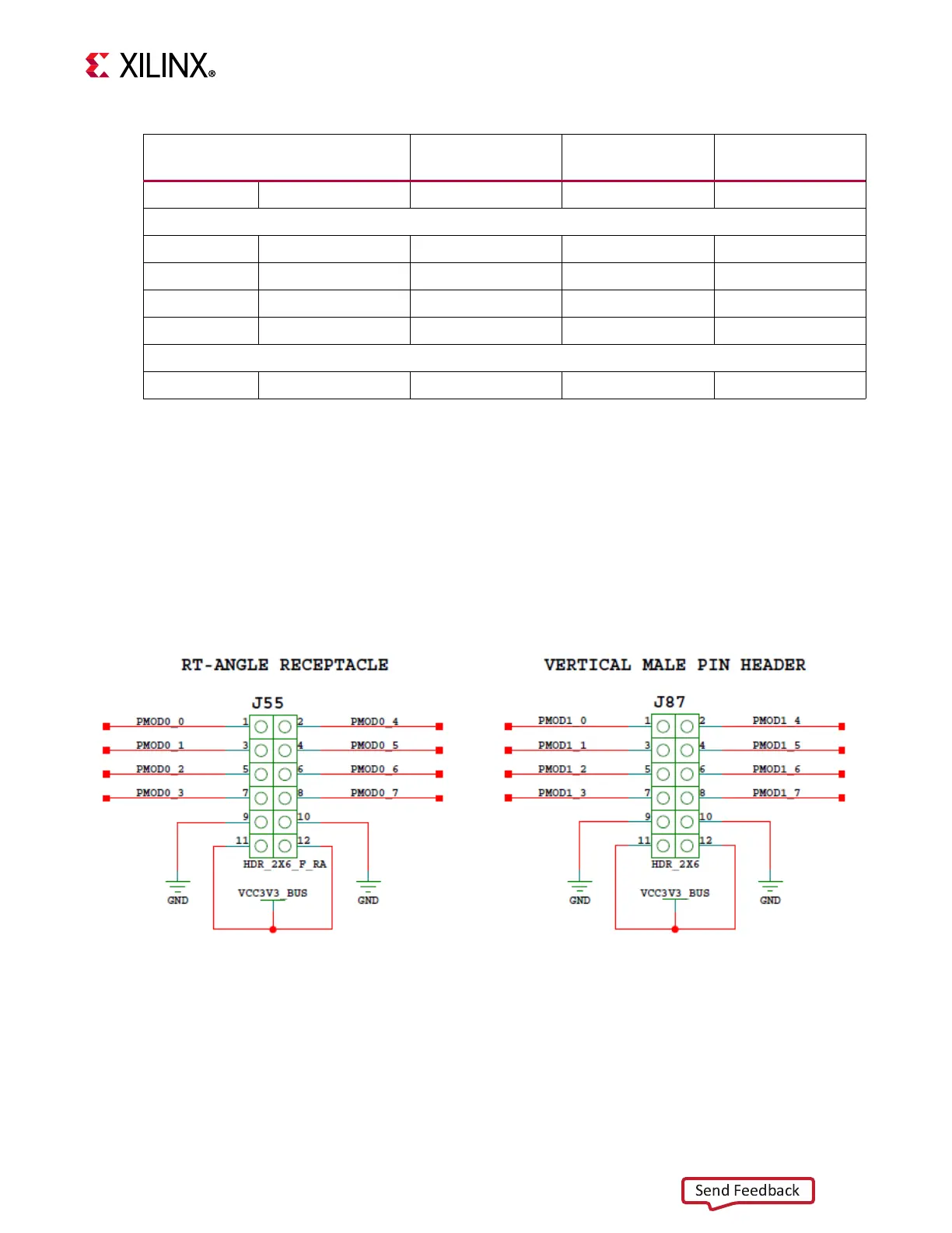
User Pmod GPIO Headers
[Figure 2-1, callout 28]
The KCU116 evaluation board supports two Pmod GPIO headers J55 and J87. The Pmod nets
are connected to FPGA U1 Bank 87. Pmod connector J55 is a right-angle receptacle and
connector J87 is a vertical male pin header.
Figure 3-25 shows the GPIO Pmod headers J55 and J87.
BANK 86 A9 GPIO_SW_C LVCMOS33 SW15.3
4-Pole DIP SW (active-High)
BANK 86 G11 GPIO_DIP_SW0 LVCMOS33 SW13.1
BANK 86 H11 GPIO_DIP_SW1 LVCMOS33 SW13.2
BANK 86 H9 GPIO_DIP_SW2 LVCMOS33 SW13.3
BANK 86 J9 GPIO_DIP_SW3 LVCMOS33 SW13.4
CPU Reset Pushbutton (active-High)
BANK 86 B9 CPU_RESET LVCMOS33 SW17.3
Table3‐20: KCU116 GPIO Connections to FPGA U1 (Cont’d)
FPGA Pin (U1)
Schematic Net
Name
I/O Standard GPIO
X-Ref Target - Figure 3-25
Figure3‐25: Pmod Connectors J52 and J53 with Level Shifters U41 and U42