KCU116 Board User Guide 41
UG1239 (v1.2) September 28, 2018 www.xilinx.com
Chapter3: Board Component Descriptions
PCI Express Endpoint Connectivity
[Figure 2-1, callout 13]
The 8-lane PCI Express edge connector P1 performs data transfers at the rate of 2.5 GT/s for
Gen1 applications, 5.0 GT/s for Gen2 applications, and 8.0 GT/s for Gen3 applications. The
PCIe transmit and receive signal data paths have a characteristic impedance of 85Ω ±10%.
The PCIe clock is routed as a 100Ω differential pair. See Table 3-7 for PCIe P1 to FPGA U1
connectivity details.
The XCKU5P-2FFVB676E device (-2 speed grade) included with the KCU116 board supports
up to Gen3 x8.
The PCIe clock is input from the P1 edge connector. It is AC coupled to FPGA U1 through the
MGTREFCLK0 pins of Quad 225. PCIE_CLK_Q0_P is connected to U1 pin V7, and the _N net
is connected to pin V6. The PCI Express clock circuit is shown in Figure 3-12.
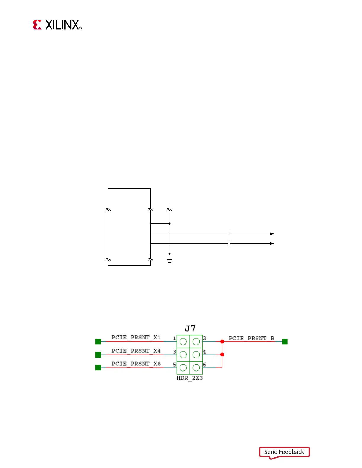
The PCIe lane width/size is selected by jumper J7 shown in Figure 3-13. The default lane size
selection is 8-lane (J7 pins 5 and 6 jumpered).
Table 3-7, page 37 lists the PCIe P1 edge connector wiring to FPGA U1.
X-Ref Target - Figure 3-12
Figure3‐12: PCI Express Clock
X-Ref Target - Figure 3-13
Figure3‐13: PCI Express Lane Size Select Jumper J7
PCI Express
Eight-Lane
Edge connector
GND
REFCLK+
REFCLK-
GND
OE
GND
A15
A14
A13
A12
P1
PCIE_CLK_Q0_C_P
PCIE_CLK_Q0_C_N
PCIE_CLK_Q0_P
PCIE_CLK_Q0_N
0.01 μF 25V
X7R
0.01 μF 25V
X7R
X18422-120916