KCU116 Board User Guide 19
UG1239 (v1.2) September 28, 2018 www.xilinx.com
Chapter3: Board Component Descriptions
DDR4 Component Memory
[Figure 2-1, callout 2]
The 1 GB DDR4 component memory system is comprised of two 512 MB DDR4 SDRAM
devices located at U150 and U153.
• Manufacturer: Micron
• Part Number: MT40A256M16GE-075E
•Description:
°
4 Gb (256 Mb x 16)
°
1.2V 96-ball TFBGA
°
DDR4-2666
The KCU116 XCKU5P FPGA DDR memory interface performance is documented in the
Kintex UltraScale+ FPGAs Data Sheet: DC and AC Switching Characteristics (DS922) [Ref 1].
This memory system is connected to the XCKU5P device HP banks 66 and 67.
The DDR4 0.6V VTT termination voltage (net DDR4_VTT) is sourced from the TI TPS51200DR
linear regulator U35. The connections between the DDR4 component memories and
XCKU5P device banks 66 and 67 are listed in Table 3-2.
The 1 GB DDR4 component memory system comprises two 512 MB DDR4 SDRAM devices
(Micron MT40A256M16GE-075E) located at U150 and U153. This memory system is
connected to the XCKU5P device HP banks 66 and 67. The DDR4 0.6V VTT termination
voltage (net DDR4_VTT) is sourced from the TI TPS51200DR linear regulator U35. The
connections between the DDR4 component memories and XCKU5P device banks 66 and 67
are listed in Table 3-2.
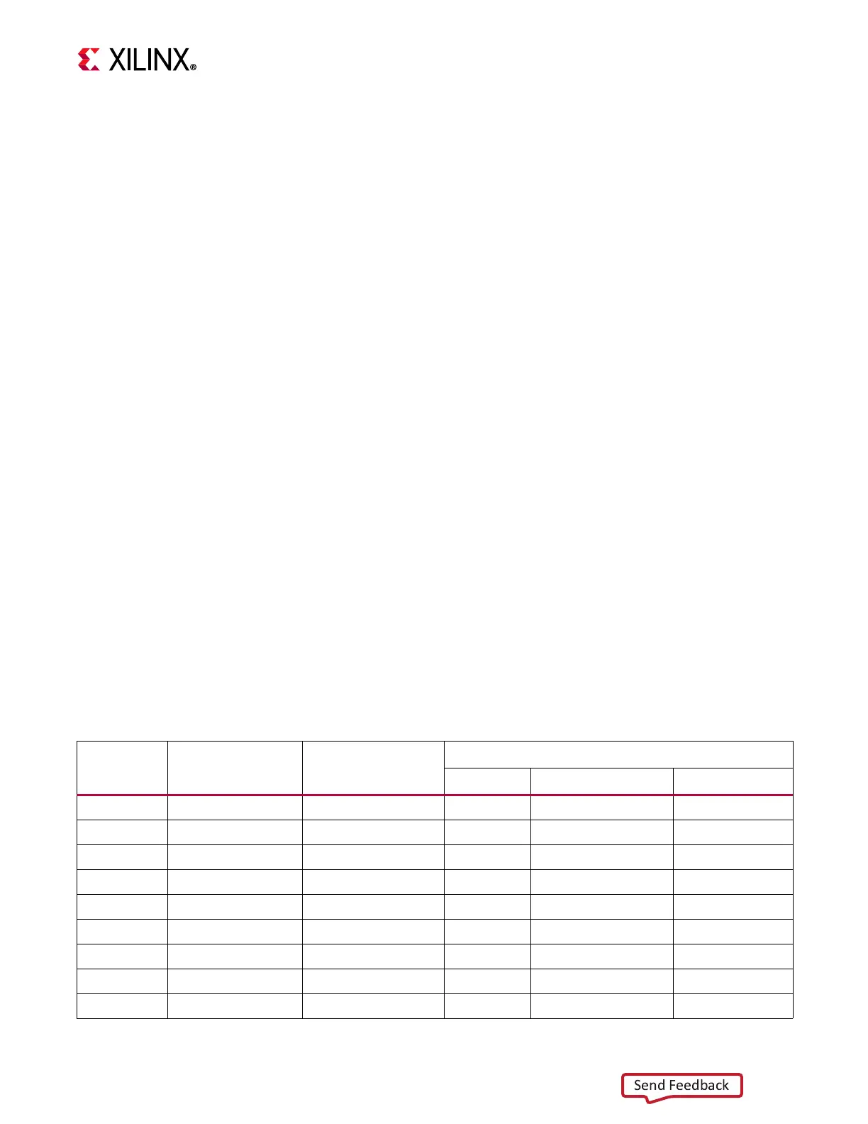
Table3‐2: DDR4 Memory Connections to the FPGA
FPGA (U1)
Pin
Schematic Net
Name
I/O Standard
Component Memory
Pin # Pin Name Ref. Des.
C22 DDR4_DQ0 POD12_DCI G2 DQL0 U150
B24 DDR4_DQ1 POD12_DCI F7 DQL1 U150
C23 DDR4_DQ2 POD12_DCI H3 DQL2 U150
A24 DDR4_DQ3 POD12_DCI H7 DQL3 U150
D21 DDR4_DQ4 POD12_DCI H2 DQL4 U150
B22 DDR4_DQ5 POD12_DCI H8 DQL5 U150
E21 DDR4_DQ6 POD12_DCI J3 DQL6 U150
A25 DDR4_DQ7 POD12_DCI J7 DQL7 U150
A19 DDR4_DQ8 POD12_DCI A3 DQU0 U150