KCU116 Board User Guide 18
UG1239 (v1.2) September 28, 2018 www.xilinx.com
Chapter3: Board Component Descriptions
I/O Voltage Rails
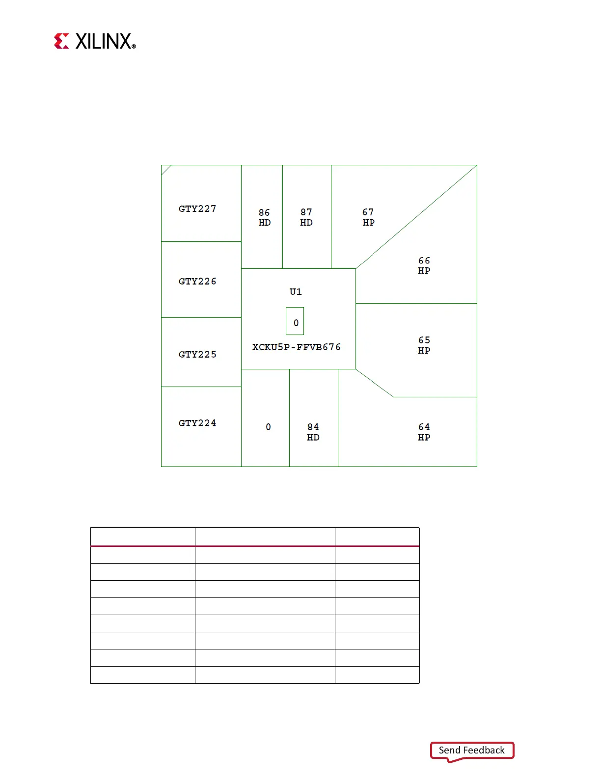
There are seven I/O banks available on the XCKU5P device and the KCU116 board. The
voltages applied to the FPGA I/O banks (shown in Figure 3-2) used by the KCU116 board are
listed in Table 3-1.
X-Ref Target - Figure 3-2
Figure3‐2: UltraScale+ XCKU5P Bank Locations
Table3‐1: I/O Bank Voltage Rails
FPGA (U1) Bank Power Supply Rail Net Name Voltage
Bank 0 VCC1V8 1.8V
HP Bank 64 VADJ_FMC 1.8V (default)
HP Bank 65 VCC1V8 1.8V
HP Bank 66 VCC1V2 1.2V
HP Bank 67 VCC1V2 1.2V
HP Bank 84 VCC3V3 3.3V
HR Bank 86 VCC3V3 3.3V
HR Bank 87 VCC3V3 3.3V