KCU116 Board User Guide 63
UG1239 (v1.2) September 28, 2018 www.xilinx.com
Chapter3: Board Component Descriptions
GPIO DIP Switch
[Figure 2-1, callout 25]
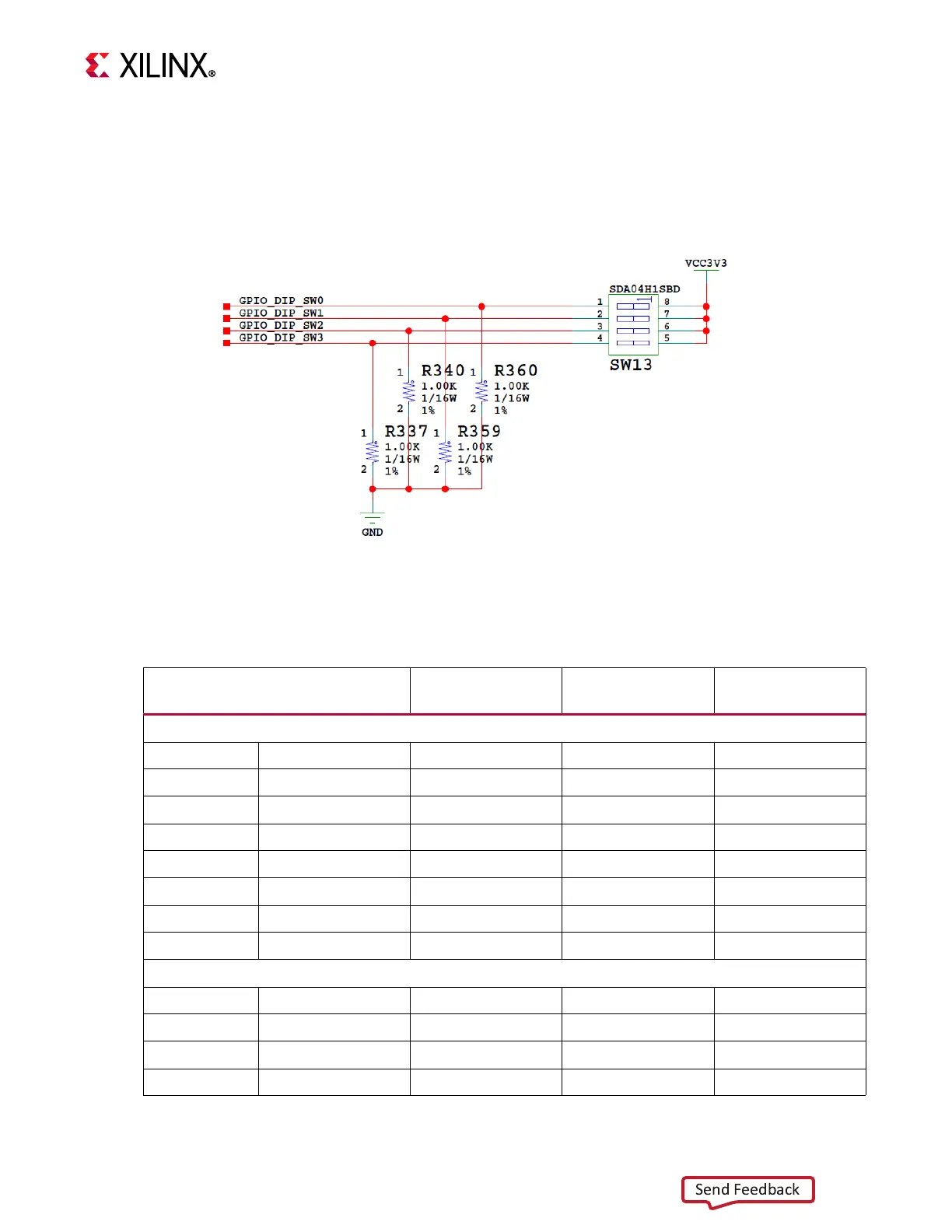
Figure 3-24 shows the GPIO DIP switch circuit.
Table 3-20 lists the GPIO connections to FPGA U1.
X-Ref Target - Figure 3-24
Figure3‐24: GPIO DIP Switch
Table3‐20: KCU116 GPIO Connections to FPGA U1
FPGA Pin (U1)
Schematic Net
Name
I/O Standard GPIO
GPIO LEDs (active-High)
BANK 86 C9 GPIO_LED_0 LVCMOS33 DS38.1
BANK 86 D9 GPIO_LED_1 LVCMOS33 DS37.1
BANK 86 E10 GPIO_LED_2 LVCMOS33 DS39.1
BANK 86 E11 GPIO_LED_3 LVCMOS33 DS40.1
BANK 86 F9 GPIO_LED_4 LVCMOS33 DS41.1
BANK 86 F10 GPIO_LED_5 LVCMOS33 DS42.1
BANK 86 G9 GPIO_LED_6 LVCMOS33 DS43.1
BANK 86 G10 GPIO_LED_7 LVCMOS33 DS44.1
Directional Pushbuttons (active-High)
BANK 86 A10 GPIO_SW_N LVCMOS33 SW18.3
BANK 86 B11 GPIO_SW_E LVCMOS33 SW22.3
BANK 86 B10 GPIO_SW_W LVCMOS33 SW14.3
BANK 86 C11 GPIO_SW_S LVCMOS33 SW16.3