KCU116 Board User Guide 33
UG1239 (v1.2) September 28, 2018 www.xilinx.com
Chapter3: Board Component Descriptions
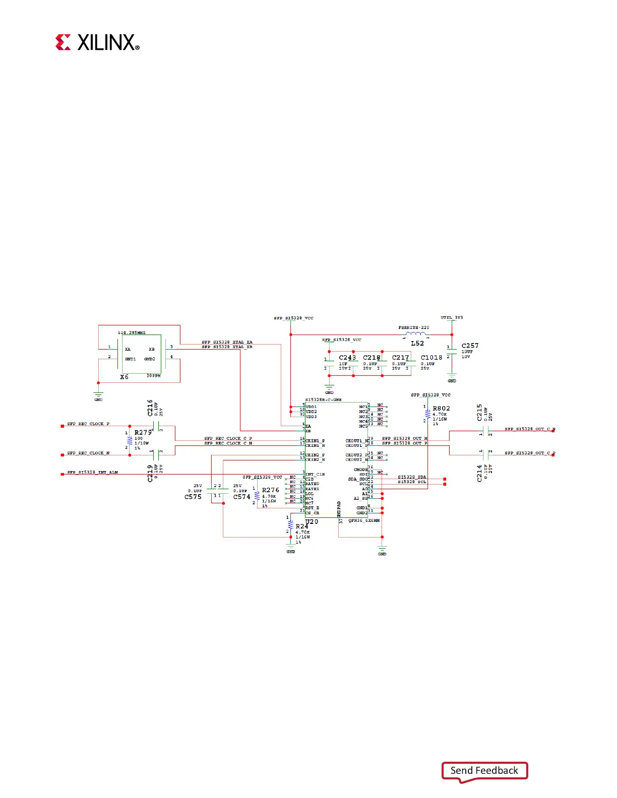
Jitter Attenuated Clock
[Figure 2-1, callout 8]
The KCU116 board includes a Silicon Labs SI5328C jitter attenuator U20. FPGA U1 user logic
can implement a clock recovery circuit and then output this clock from a differential pair on
I/O bank 84 (SFP_REC_CLOCK_P, FPGA U1 pin AB15 and SFP_REC_CLOCK_N, U1 pin AAB16)
for jitter attenuation. The jitter attenuated clock (SFP_SI5328_OUT_P (U20 pin 28),
SFP_SI5328_OUT_N (U20 pin 29)) is then routed as a series capacitor coupled reference
clock to GTY Quad 226 inputs MGTREFCLK1P (U1 pin M7) and MGTREFCLK1N (U1 pin M6).
The primary purpose of this clock is to support common packet radio interface (CPRI™) or
open base station architecture initiative (OBSAI) applications. These applications perform
clock recovery from a user-supplied small form-factor pluggable (SFP/SFP+) module, and
use the jitter attenuated recovered clock to drive the reference clock inputs of a GTH
transceiver. The jitter attenuated clock is shown in Figure 3-9.
X-Ref Target - Figure 3-9
Figure3‐9: Jitter Attenuated Clock