KCU116 Board User Guide 26
UG1239 (v1.2) September 28, 2018 www.xilinx.com
Chapter3: Board Component Descriptions
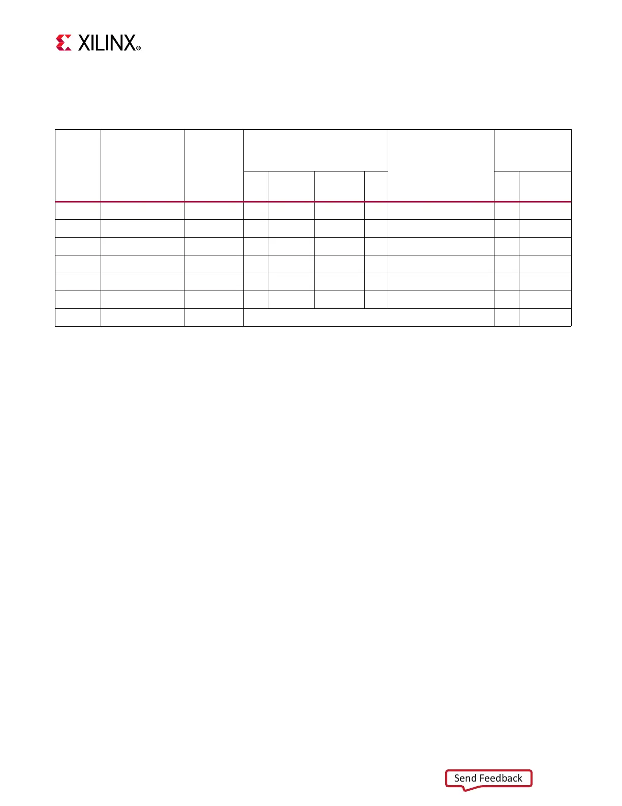
The connections between the SD card connector and system controller U161 are listed in
Table 3-4.
For more information on secure digital nonvolatile memory card technology, see the
SanDisk [Ref 24] and SD Association [Ref 25] websites.
USB JTAG Interface
[Figure 2-1, callout 5]
JTAG configuration is provided through a Digilent onboard USB-to-JTAG configuration
logic module (U21), in which a host computer accesses the KCU116 board JTAG chain
through a type-A (host side) to micro-B (KCU116 board side J2) USB cable.
A 2 mm JTAG header (J8) is also provided in parallel for access by Xilinx
®
download cables,
such as the Platform Cable USB II and the Parallel Cable IV. JTAG configuration is allowed at
any time regardless of the FPGA mode pin settings. JTAG initiated configuration takes
priority over the configuration method selected through the FPGA mode pin M2 (which is
wired to DIP SW21 pin 6, switch position 6). The JTAG chain of the KCU116 board is shown
in Figure 3-5. For more details about the Digilent USB JTAG module, see the Digilent
website [Ref 26].
Table3‐4: SD Card Connections to System Controller U161
XC7Z010
(U161)
Schematic Net
Name
I/O
Standard
Level Shifter (U178)
Schematic Net Name
SDIO
Connector
(J177)
Pin
#
Pin
Name
Pin Name
Pin
#
Pin
#
Pin Name
D6 SDIO_DATA0 LVCMOS18 1 IO_VL1 IO_VCC1 15 SDIO_CONN_DATA0 7 DAT0
C6 SDIO_DATA1 LVCMOS18 3 IO_VL2 IO_VCC2 5 SDIO_CONN_DATA1 8 DAT1
B9 SDIO_DATA2 LVCMOS18 4 IO_VL3 IO_VCC3 6 SDIO_CONN_DATA2 1 DAT2
D10 SDIO_DATA3 LVCMOS18 9 IO_VL4 IOVCC4 7 SDIO_CONN_DATA3 2 CD_DAT3
B10 DIO_CMD LVCMOS18 10 IO_VL5 IO_VCC5 8 SDIO_CONN_CMD 3 CMD
B7 SDIO_CLK LVCMOS18 12 CLK_VL CLK_VCC 14 SDIO_CONN_CLK 5 CLK
D8 SDIO_CONN_CD LVCMOS18 Direct Connect 13 DETECT