KCU116 Board User Guide 61
UG1239 (v1.2) September 28, 2018 www.xilinx.com
Chapter3: Board Component Descriptions
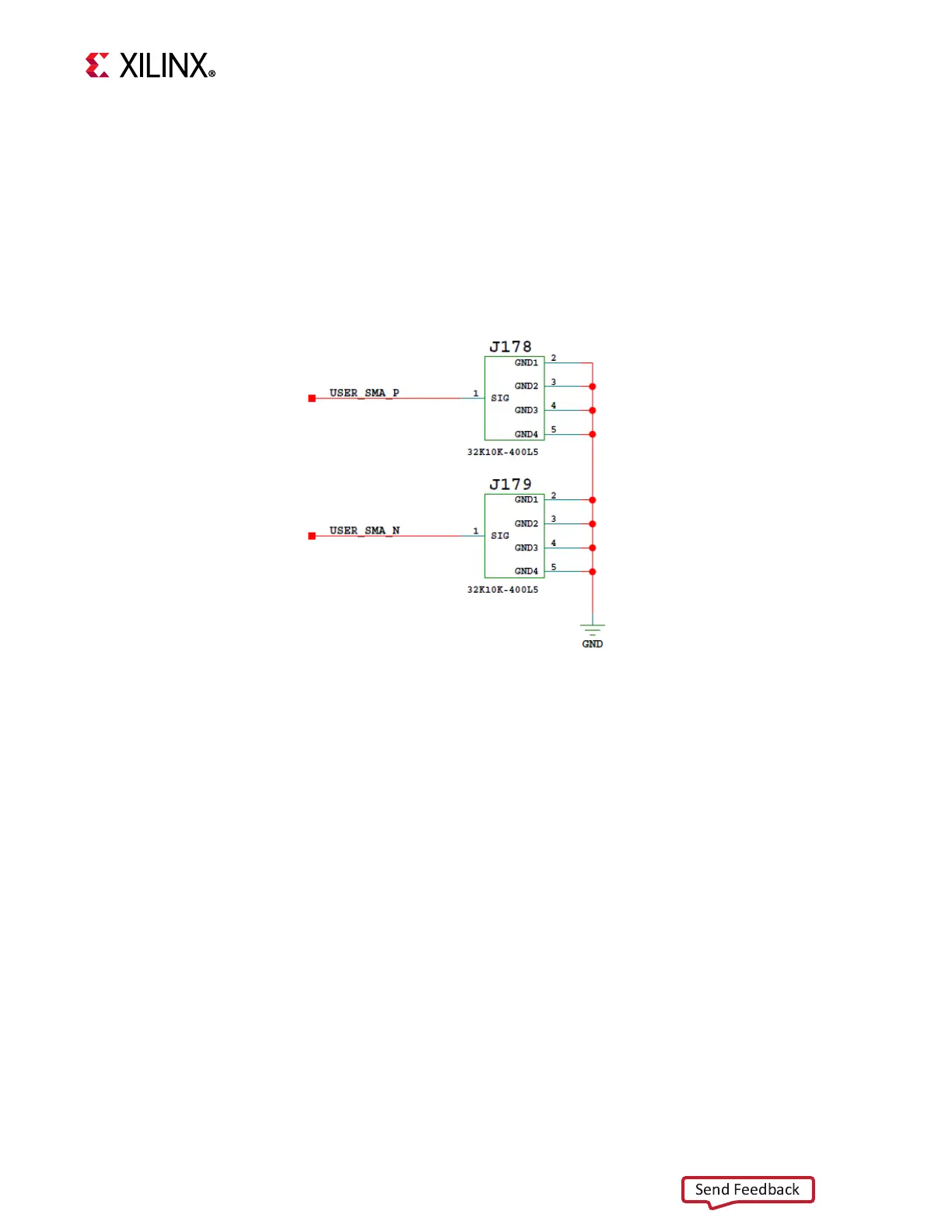
User SMA GPIO
[Figure 2-1, callout 10]
The KCU116 board provides a pair of SMAs for differential user I/O into FPGA U1 bank 66
(see Figure 3-22). The P-side SMA J178 signal USER_SMA_P is connected to U1 pin K25, and
the N-side SMA J179 signal USER_SMA_N is connected to U1 pin K26. Bank 66
VCCO
is 1.2V
VCC1V2. The USER_SMA_CLOCK input voltage swing should not exceed 1.2V.
X-Ref Target - Figure 3-22
Figure3‐22: User SMA GPIO