KCU116 Board User Guide 23
UG1239 (v1.2) September 28, 2018 www.xilinx.com
Chapter3: Board Component Descriptions
Dual Quad SPI Flash Memory
[Figure 2-1, callout 3]
The Quad SPI flash memory located at U2 and U3 provides 2 x 1 Gb of nonvolatile storage
that can be used for configuration and data storage.
• Part number: MT25QU01GBBB8ESF-0SIT (Micron)
• Supply voltage: 1.8V
• Datapath width: 8 bits
• Data rate: variable, depending on single, dual, or quad mode and whether the EMCCLK
or the internal CCLK is used (bitstream configurable). See UltraScale Architecture
Configuration User Guide (UG570) [Ref 3] for more information.
The connections between the SPI flash memories and the XCKU5P device are listed in
Table 3-3.
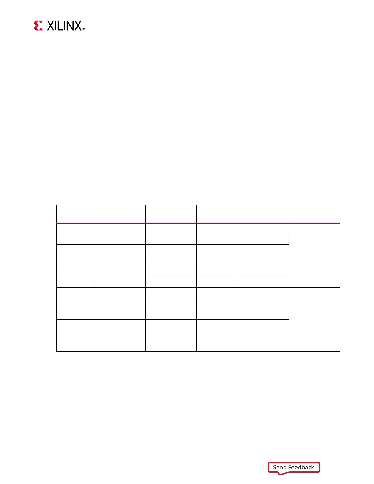
Table3‐3: Quad SPI Flash Memory Connections to FPGA U1
FPGA (U1)
Pin
Schematic Net
Name
I/O Standard Pin Number Pin Name Ref. Des.
AD11 QSPI0_DQ0 LVCMOS18 15 DQ0
U2
AC12 QSPI0_DQ1 LVCMOS18 8 DQ1
AC11 QSPI0_DQ2 LVCMOS18 9 DQ2/VPP/WP_B
AE11 QSPI0_DQ3 LVCMOS18 1 DQ3/HOLD_B
Y11 QSPI_CLK See Note 1 16 C
AA12 QSPI0_CS_B LVCMOS18 7 S_B
N19 QSPI1_DQ0 LVCMOS18 15 DQ0
U3
P23 QSPI1_DQ1 LVCMOS18 8 DQ1
N23 QSPI1_DQ2 LVCMOS18 9 DQ2/VPP/WP_B
R21 QSPI1_DQ3 LVCMOS18 1 DQ3/HOLD_B
Y11 QSPI_CLK
(1)
16 C
R20 QSPI1_CS_B LVCMOS18 7 S_B
Notes:
1. For details on bank 0 pins, see the UltraScale Architecture Configuration User Guide (UG570) [Ref 3].