KCU116 Board User Guide 30
UG1239 (v1.2) September 28, 2018 www.xilinx.com
Chapter3: Board Component Descriptions
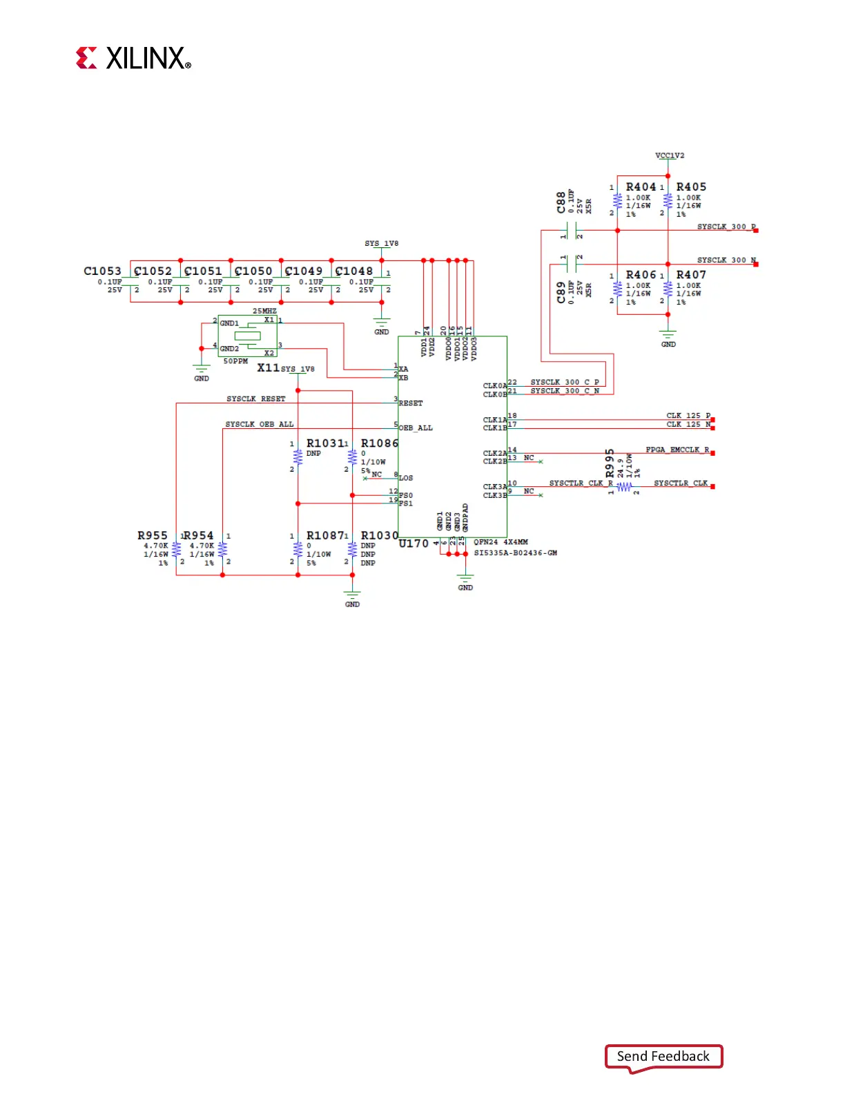
The system clock circuit is shown in Figure 3-6.
Three additional clocks are sourced from the U170 quad clock generator:
• 125 MHz LVDS signal pair CLK_125MHZ_P and CLK_125MHZ_N, connected to XCKU5P
FPGA U1 bank 87 pins G12 and F12, respectively.
• 90.0 MHz single-ended 1.8V LVCMOS, series resistor coupled FPGA_EMCCLK,
connected to XCKU5P FPGA U1 bank 65 dedicated EMCCLK input pin N21.
• 33.3333 MHz single-ended 1.8V LVCMOS, series resistor coupled SYSCTLR_CLK,
connected to system controller XC7Z010 Zynq-7000 SoC U161 bank 500 dedicated
PS_CLK input pin C7.
X-Ref Target - Figure 3-6
Figure3‐6: KCU116 System Clock