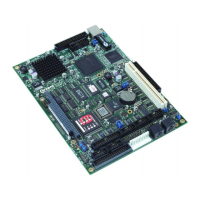
SBC-GX1 Technical Manual Appendix G – Display Converter 1 (DC1)
Setting the Voltage Range
The minimum voltage is controlled by the value of resistor R23.
V
FB
= 1.25V
V
OUT(MIN)
= required minimum voltage (minimum possible is 12V)
()
FB
FBMINOUT
V
VV
R
−×
=
)(
3
10120
23
The maximum voltage is controlled by the value of the resistor R18.
V
FB =
1.25V
V
OUT(MAX)
= required maximum voltage (maximum possible is 27.5V)V
OUT(MIN)
= Voltage
used to determine the value of R23.
)()(
23
18
MINOUTMAXOUT
FB
VV
VR
R
−
×
=
On power up the MAX686 resets to the mid-scale output voltage. This value can be
calculated as follows:
()
18
23
635.0
)()(
R
R
VVV
FBMINOUTMIDOUT
×−+=
Configuring the CS9211
Once the connections are made and the SBC-GX1 is powered up the CS9211 must be
configured to drive the display. This can either be achieved by running a separate
application program or can be included in the operating system drivers. The DC1 has
been used with DOS, Windows CE and VxWorks, and an example ‘C’ application is
provided showing the settings required.
In order to achieve the optimum display for your application it may be necessary to
adjust some of the CS9211 parameters. The differing and frame rate settings should be
set at appropriate values for the image that is going to be displayed. Details on these
settings can be found in the National Semiconductors CS9211 data sheet.
As the display is configured after the board has loaded an operating system,
there will be no output on the display until this time. Therefore a CRT display
may be used to ensure that the board is configured correctly.
If any of the BIOS setup parameters need to be adjusted then the CRT will be
required as entering the BIOS is achieved in the initial POST process.
© 2004 Arcom Issue D 103

 Loading...