TIME PROCESSOR UNIT MC68332
7-12 USER’S MANUAL
7.6.1 System Configuration Registers
The TPU configuration control registers, TPUMCR and TICR, determine the value of
the prescaler, perform emulation control, specify whether the external TCR2 pin func-
tions as a clock source or as gate of the DIV8 clock for TCR2, and determine interrupt
request level and interrupt vector number assignment. Refer to APPENDIX D REGIS-
TER SUMMARY for more information about TPUMCR and TICR.
7.6.1.1 Prescaler Control for TCR1
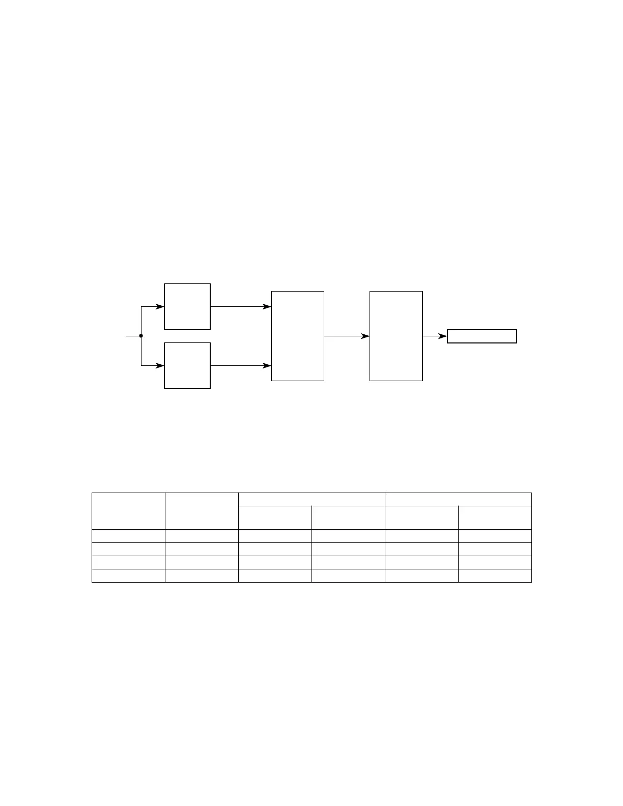
Timer control register one (TCR1) is clocked from the output of a prescaler. Two fields
in the TPUMCR control TCR1. The prescaler's input is the internal TPU system clock
divided by either 4 or 32, depending on the value of the PSCK (prescaler clock) bit.
The prescaler divides this input by 1, 2, 4, or 8, depending on the value of TCR1P (tim-
er count register 1 prescaler control). Channels using TCR1 have the capability to re-
solve down to the TPU system clock divided by 4. Refer to Figure 7-2 and Table 7-1.
Figure 7-2 TCR1 Prescaler Control
7.6.1.2 Prescaler Control for TCR2
Timer control register two (TCR2), like TCR1, is clocked from the output of a prescaler.
The T2CG (TCR2 clock/gate control) bit in TPUMCR determines whether the external
TCR2 pin functions as an external clock source for TCR2 or as the gate in the use of
TCR2 as a gated pulse accumulator. The function of the T2CG bit is shown in Figure
7-3.
Table 7-1 TCR1 Prescaler Control
PSCK = 0 PSCK = 1
TCR1 Prescaler Divide
By
Number of
Clocks
Rate at
16 MHz
Number of
Clocks
Rate at
16 MHz
00 1 32 2 ms 4 250 ns
01 2 64 4 ms 8 500 ns
10 4 128 8 ms 16 1 ms
11 8 256 16 ms 32 2 ms
TCR1
015
PSCK
MUX
÷ 4
DIV4 CLOCK
÷ 32
DIV32 CLOCK
TCR1
PRESCALER
00 ÷ 1
01 ÷ 2
10 ÷ 4
11 ÷ 8
SYSTEM
CLOCK
1 – DIV4
0 – DIV32
PRESCALER CTL BLOCK 1
Fr
ees
cale S
em
iconduct
or
, I
Freescale Semiconductor, Inc.
For More Information On This Product,
Go to: www.freescale.com
nc...