MC68332 REGISTER SUMMARY
USER’S MANUAL D-9
D.2.9 PORTF0/PORTF1 — Port F Data Register $YFFA19, $YFFA1B
PORTF is an internal data latch that can be accessed at two locations. It can be read
or written at any time. If a pin in I/O port F is configured as an output, the corresponding
bit value is driven out on the pin. When a pin is configured for output, a read of PORTF
returns the latched bit value; when a pin is configured for input, a read returns the pin
logic level.
D.2.10 DDRF — Port F Data Direction Register $YFFA1D
Bits in this register control the direction of the port F pin drivers when pins are config-
ured for I/O. Setting a bit configures the corresponding pin as an output; clearing a bit
configures the corresponding pin as an input. This register can be read or written at
any time.
D.2.11 PFPAR — Port F Pin Assignment Register $YFFA1F
Bits in this register determine the function of port F pins. Setting a bit assigns the cor-
responding pin to a control signal; clearing a bit assigns the pin to port F.
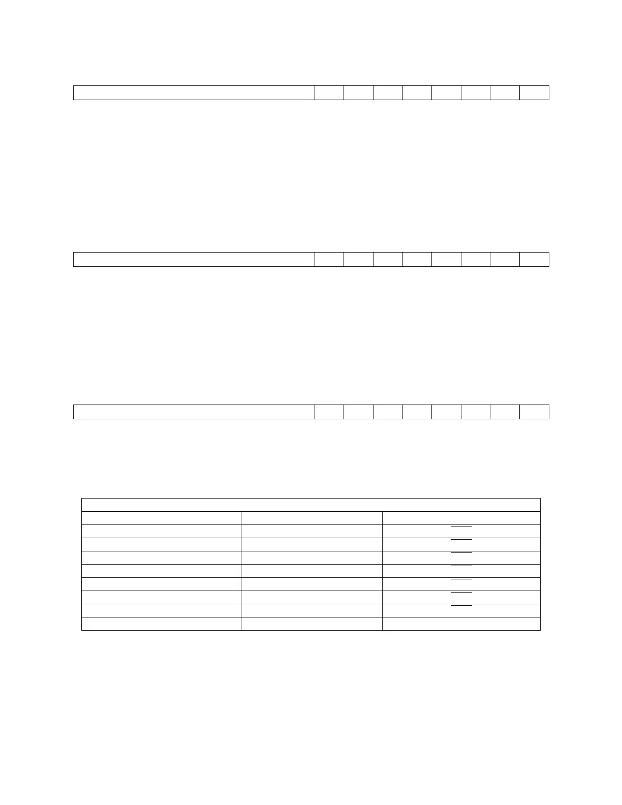
15 8 7 6 5 4 3 2 1 0
NOT USED PF7 PF6 PF5 PF4 PF3 PF2 PF1 PF0
RESET:
U U U U U U U U
15 8 7 6 5 4 3 2 1 0
NOT USED DDF7 DDF6 DDF5 DDF4 DDF3 DDF2 DDF1 DDF0
RESET:
0 0 0 0 0 0 0 0
15 8 7 6 5 4 3 2 1 0
NOT USED PFPA7 PFPA6 PFPA5 PFPA4 PFPA3 PFPA2 PFPA1 PFPA0
RESET:
DATA9 DATA9 DATA9 DATA9 DATA9 DATA9 DATA9 DATA9
Port F Pin Assignments
PFPAR Field Port F Signal Control Signal
PFPA7 PF7 IRQ7
PFPA6 PF6 IRQ6
PFPA5 PF5 IRQ5
PFPA4 PF4 IRQ4
PFPA3 PF3 IRQ3
PFPA2 PF2 IRQ2
PFPA1 PF1 IRQ1
PFPA0 PF0 MODCLK
Fr
ees
cale S
em
iconduct
or
, I
Freescale Semiconductor, Inc.
For More Information On This Product,
Go to: www.freescale.com
nc...