REGISTER SUMMARY MC68332
D-14 USER’S MANUAL
BLKSZ — Block Size
This field determines the size of the block above the base address that is enabled by
the chip select.
D.2.27 CSORBT — Chip Select Option Register Boot ROM $YFFA4A
D.2.28 CSOR[0:10] — Chip Select Option Registers $YFFA4E–$YFFA76
Contain parameters that support bootstrap operations from peripheral memory devic-
es. Bit and field definitions for CSORBT and CSOR[0:10] are the same.
MODE — Asynchronous Bus/Synchronous E-Clock Mode
Synchronous mode cannot be used with internally generated autovectors.
0 = Asynchronous mode selected
1 = Synchronous mode selected
BYTE — Upper/Lower Byte Option
The value in this field determines whether a select signal can be asserted.
R/W
— Read/Write
This field causes a chip select to be asserted only for a read, only for a write, or for
both read and write.
STRB — Address Strobe/Data Strobe
0 = Address strobe
1 = Data strobe
DSACK
— Data Strobe Acknowledge
This field specifies the source of DSACK
in asynchronous bus mode and controls wait
state insertion.
SPACE — Address Space Select
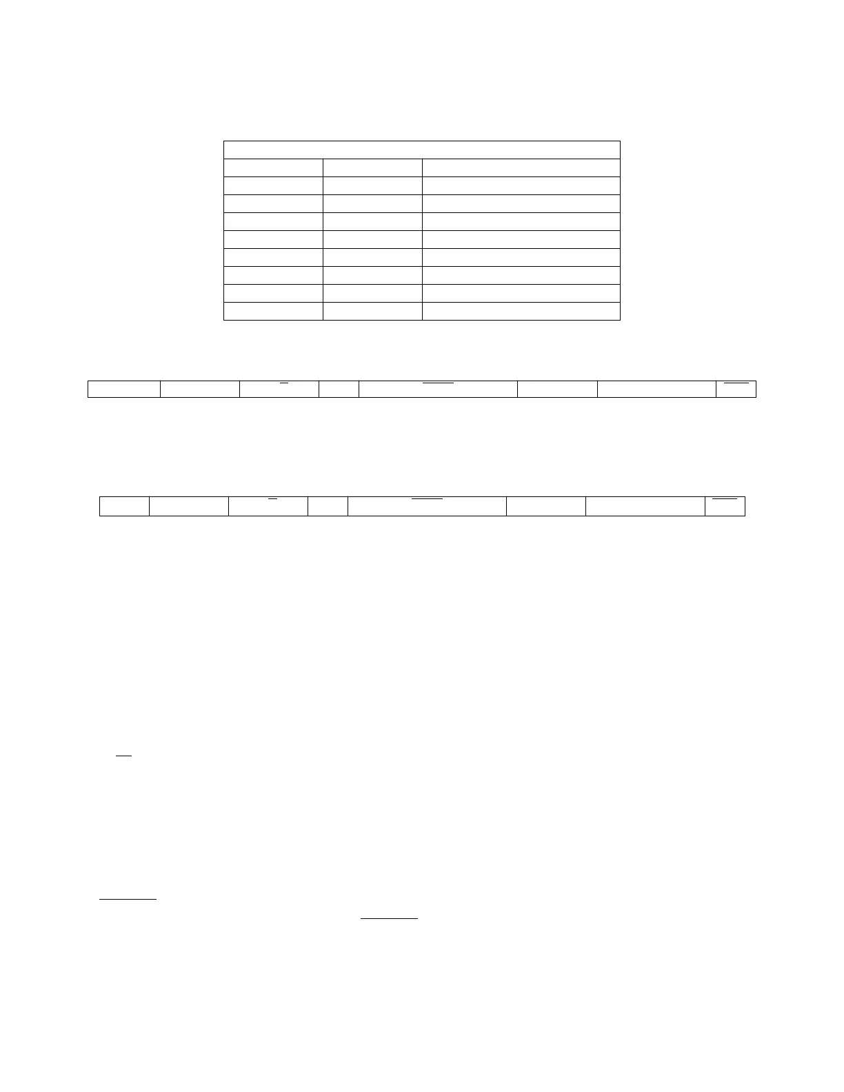
Block Size Encoding
BLKSZ[2:0] Block Size Address Lines Compared
000 2 K ADDR[23:11]
001 8 K ADDR[23:13]
010 16 K ADDR[23:14]
011 64 K ADDR[23:16]
100 128 K ADDR[23:17]
101 256 K ADDR[23:18]
110 512 K ADDR[23:19]
111 1 M ADDR[23:20]
15 14131211109 6543 10
MODE BYTE R/W
STRB DSACK SPACE IPL AVEC
RESET:
0 111101101110000
15 14 13 12 11 10 9 6 5 4 3 1 0
MODE BYTE R/W STRB DSACK SPACE IPL AVEC
RESET:
0 0 0 0 0 0 0 0 0 0 0 0 0 0 0 0
Fr
ees
cale S
em
iconduct
or
, I
Freescale Semiconductor, Inc.
For More Information On This Product,
Go to: www.freescale.com
nc...