MC68332 REGISTER SUMMARY
USER’S MANUAL D-13
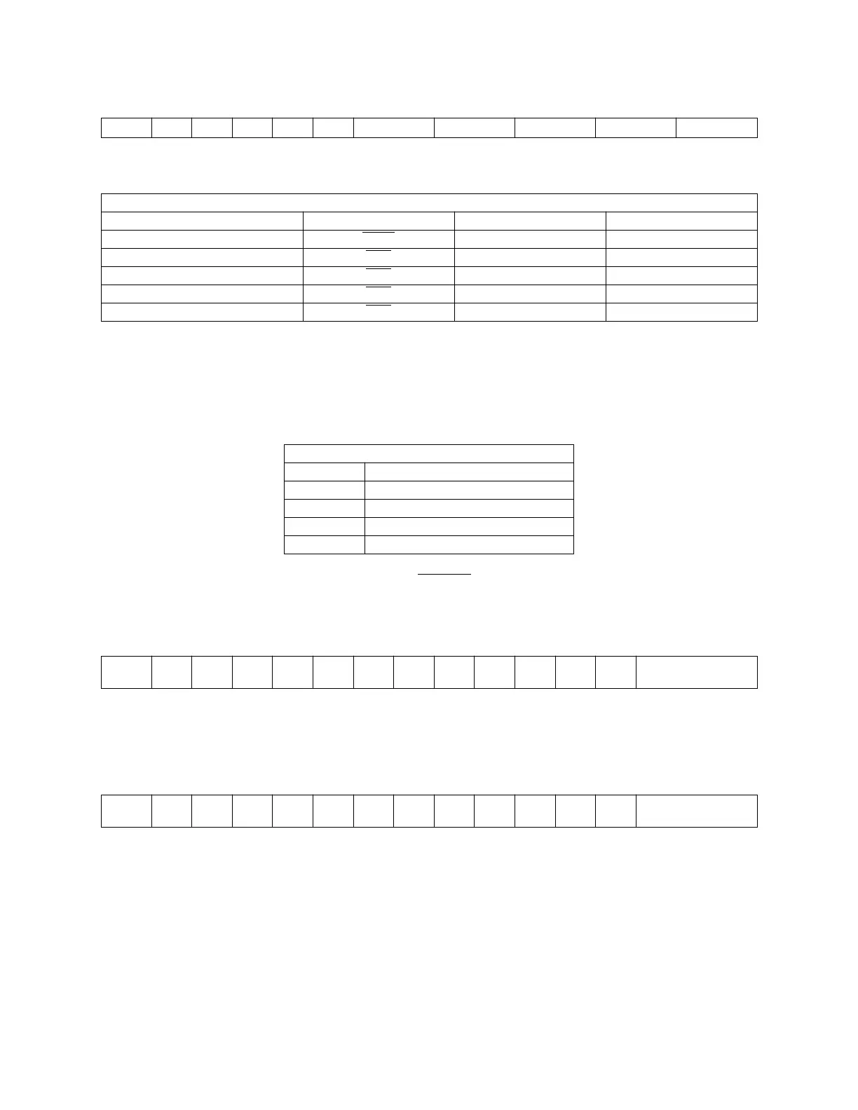
D.2.24 CSPAR1 — Chip Select Pin Assignment Register 1 $YFFA46
Contains five 2-bit fields (CSPA1[4:0]) that determine the functions of corresponding
chip-select pins. CSPAR1[15:10] are not used. These bits always read zero; write has
no effect. The CSPAR1 pin assignments table shows alternate functions that can be
enabled by data bus mode selection during reset.
*Does not apply to the CSBOOT field
D.2.25 CSBARBT — Chip Select Base Address Register Boot ROM $YFFA48
D.2.26 CSBAR[0:10] — Chip Select Base Address Registers $YFFA4C–$YFFA74
Each chip-select pin has an associated base address register. A base address is the
lowest address in the block of addresses enabled by a chip select. CSBARBT contains
the base address for selection of a bootstrap peripheral memory device. Bit and field
definition for CSBARBT and CSBAR[0:10] are the same, but reset block sizes differ.
ADDR[23:11] — Base Address
This field sets the starting address of a particular address space.
15 14 13 12 11 10 9 8 7 6 5 4 3 2 1 0
0 0 0 0 0 0 CSPA1[4] CSPA1[3] CSPA1[2] CSPA1[1] CSPA1[0]
RESET:
0 0 0 0 0 0 DATA7 1 DATA6 1 DATA5 1 DATA4 1 DATA3 1
CSPAR1 Pin Assignments
CSPAR1 Field CSPAR1 Signal Alternate Signal Discrete Output
CSPA1[4] CS10
ADDR23 ECLK
CSPA1[3] CS9
ADDR22 PC6
CSPA1[2] CS8
ADDR21 PC5
CSPA1[1] CS7
ADDR20 PC4
CSPA1[0] CS6
ADDR19 PC3
Pin Assignment Field Encoding
Bit Field Description
00 Discrete Output*
01 Alternate Function*
10 Chip Select (8-Bit Port)
11 Chip Select (16-Bit Port)
15 14 13 12 11 10 9 8 7 6 5 4 3 2 0
ADDR
23
ADDR
22
ADDR
21
ADDR
20
ADDR
19
ADDR
18
ADDR
17
ADDR
16
ADDR
15
ADDR
14
ADDR
13
ADDR
12
ADDR
11
BLKSZ
RESET:
0 0 0 0 0 0 0 0 0 0 0 0 0 1 1 1
15 14 13 12 11 10 9 8 7 6 5 4 3 2 0
ADDR
23
ADDR
22
ADDR
21
ADDR
20
ADDR
19
ADDR
18
ADDR
17
ADDR
16
ADDR
15
ADDR
14
ADDR
13
ADDR
12
ADDR
11
BLKSZ
RESET:
0 0 0 0 0 0 0 0 0 0 0 0 0 0 0 0
Fr
ees
cale S
em
iconduct
or
, I
Freescale Semiconductor, Inc.
For More Information On This Product,
Go to: www.freescale.com
nc...