REGISTER SUMMARY MC68332
D-12 USER’S MANUAL
D.2.18 TSTSC — Test Module Shift Count $YFFA34
Register is used for factory test only.
D.2.19 TSTRC — Test Module Repetition Count $YFFA36
Register is used for factory test only.
D.2.20 CREG — Test Submodule Control Register $YFFA38
Register is used for factory test only.
D.2.21 DREG — Distributed Register $YFFA3A
Register is used for factory test only.
D.2.22 PORTC — Port C Data Register $YFFA41
PORTC latches data for chip-select pins that are used for discrete output.
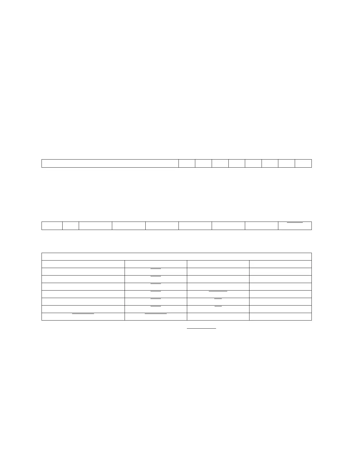
D.2.23 CSPAR0 — Chip Select Pin Assignment Register 0 $YFFA44
Contains seven 2-bit fields, CSPA0[6:1] and CSBOOT
, that determine the functions of
corresponding chip-select pins. CSPAR0[15:14] are not used. These bits always read
zero; write has no effect. CSPAR0 bit 1 always reads one; writes to CSPAR0 bit 1 have
no effect. The alternate functions can be enabled by data bus mode selection during
reset.
15 8 7 6 5 4 3 2 1 0
NOT USED 0 PC6 PC5 PC4 PC3 PC2 PC1 PC0
RESET:
0 1 1 1 1 1 1 1
15 14 13 12 11 10 9 8 7 6 5 4 3 2 1 0
0 0 CSPA0[6] CSPA0[5] CSPA0[4] CSPA0[3] CSPA0[2] CSPA0[1] CSBOOT
RESET:
0 0 DATA2 1 DATA2 1 DATA2 1 DATA1 1 DATA1 1 DATA1 1 1 DATA0
CSPAR0 Pin Assignments
CSPAR0 Field CSPAR0 Signal Alternate Signal Discrete Output
CSPA0[6] CS5
FC2 PC2
CSPA0[5] CS4
FC1 PC1
CSPA0[4] CS3
FC0 PC0
CSPA0[3] CS2
BGACK —
CSPA0[2] CS1
BG —
CSPA0[1] CS0
BR —
CSBOOT
CSBOOT ——
Fr
ees
cale S
em
iconduct
or
, I
Freescale Semiconductor, Inc.
For More Information On This Product,
Go to: www.freescale.com
nc...