MC68332 REGISTER SUMMARY
USER’S MANUAL D-25
DDRQS determines the direction of the TXD pin only when the SCI transmitter is dis-
abled. When the SCI transmitter is enabled, the TXD pin is an output.
D.4.10 SPCR0 — QSPI Control Register 0 $YFFC18
SPCR0 contains parameters for configuring the QSPI and enabling various modes of
operation. The CPU has read/write access to SPCR0, but the QSM has read access
only. SPCR0 must be initialized before QSPI operation begins. Writing a new value to
SPCR0 while the QSPI is enabled disrupts operation.
MSTR — Master/Slave Mode Select
0 = QSPI is a slave device.
1 = QSPI is system master.
NOTES:
1. PQS2 is a digital I/O pin unless the SPI is enabled (SPE in SPCR1 set), in which case it becomes
SPI serial clock SCK.
2. PQS7 is a digital I/O pin unless the SCI transmitter is enabled (TE in SCCR1 set), in which case
it becomes SCI serial output TXD.
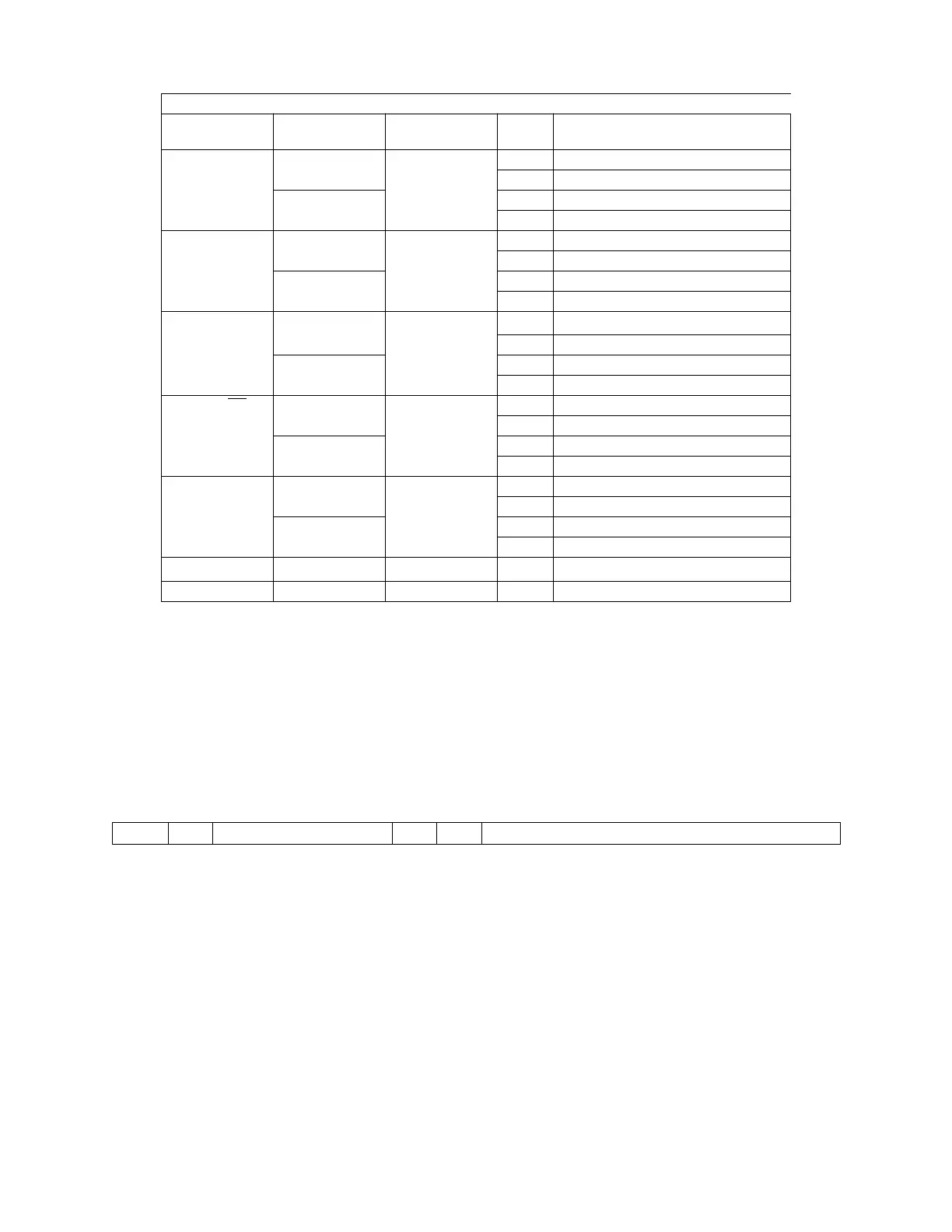
Effect of DDRQS on QSM Pin Function
QSM Pin Mode DDRQS Bit Bit
State
Pin Function
MISO Master DDQS0 0 Serial Data Input to QSPI
1 Disables Data Input
Slave 0 Disables Data Output
1 Serial Data Output from QSPI
MOSI Master DDQS1 0 Disables Data Output
1 Serial Data Output from QSPI
Slave 0 Serial Data Input to QSPI
1 Disables Data Input
SCK
1
Master DDQS2 0 Disables Clock Output
1 Clock Output from QSPI
Slave 0 Clock Input to QSPI
1 Disables Clock Input
PCS0/SS
Master DDQS3 0 Assertion Causes Mode Fault
1 Chip-Select Output
Slave 0 QSPI Slave Select Input
1 Disables Select Input
PCS[3:1] Master DDQS 0 Disables Chip-Select Output
[4:6] 1 Chip-Select Output
Slave 0 Inactive
1 Inactive
TXD
2
Transmit DDQS7 X Serial Data Output from SCI
RXD Receive None NA Serial Data Input to SCI
15 14 13 10 9 8 7 0
MSTR WOMQ BITS CPOL CPHA SP
RESET:
0 0 0 0 0 0 0 1 0 0 0 0 0 1 0 0
Fr
ees
cale S
em
iconduct
or
, I
Freescale Semiconductor, Inc.
For More Information On This Product,
Go to: www.freescale.com
nc...