REGISTER SUMMARY MC68332
D-24 USER’S MANUAL
DDRQS determines whether pins are inputs or outputs. Clearing a bit makes the cor-
responding pin an input; setting a bit makes the pin an output. DDRQS affects both
QSPI function and I/O function.
NOTES:
1. PQS2 is a digital I/O pin unless the SPI is enabled (SPE in
SPCR1 set), in which case it becomes SPI serial clock SCK
2. PQS7 is a digital I/O pin unless the SCI transmitter is enabled
(TE in SCCR1 set), in which case it becomes SCI serial output
TXD.
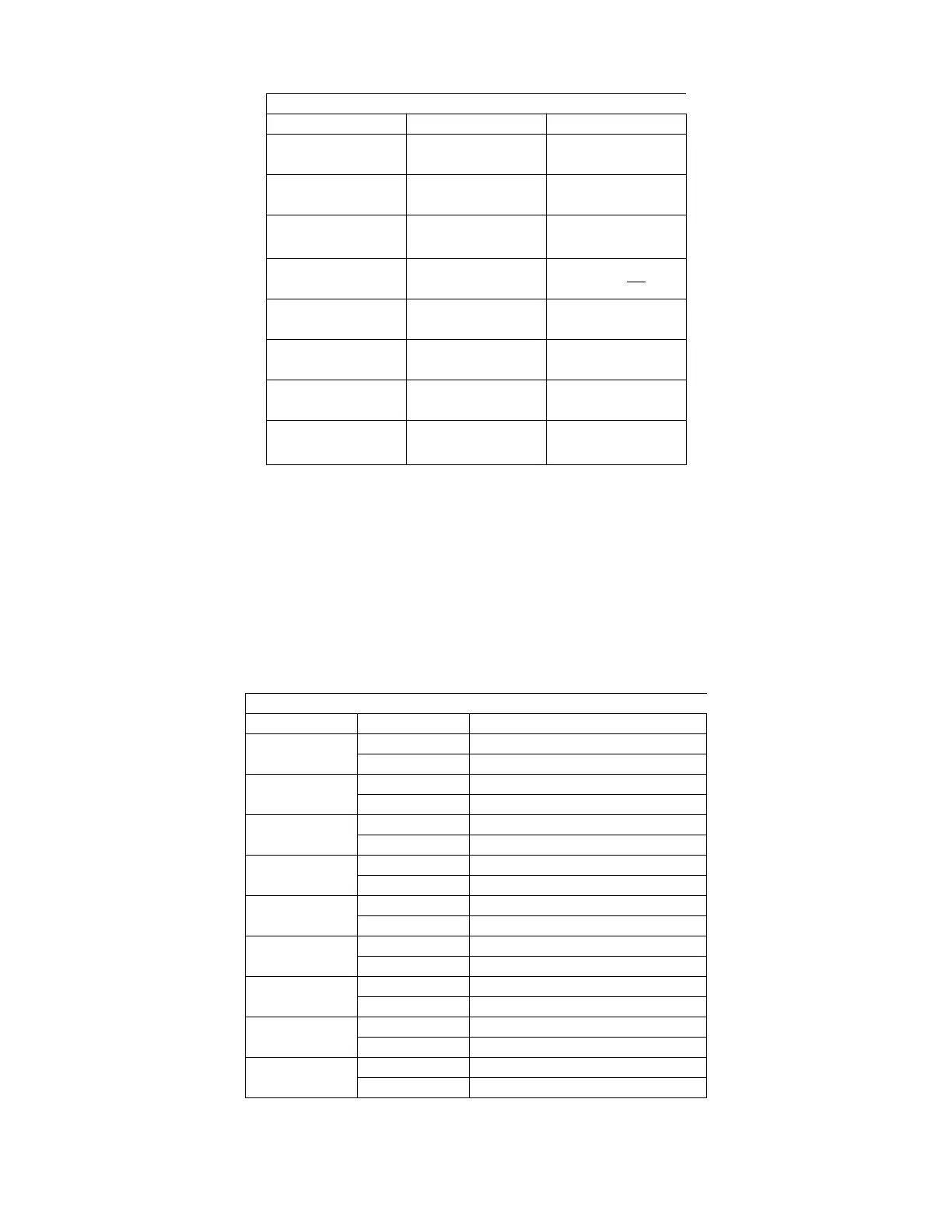
PQSPAR Pin Assignments
PQSPAR Field PQSPAR Bit Pin Function
PQSPA0 0 PQS0
1 MISO
PQSPA1 0 PQS1
1 MOSI
PQSPA2 0
PQS2
1
1 SCK
PQSPA3 0 PQS3
1 PCS0/SS
PQSPA4 0 PQS4
1 PCS1
PQSPA5 0 PQS5
1 PCS2
PQSPA6 0 PQS6
1 PCS3
PQSPA7 0
PQS7
2
1 TXD
Effect of DDRQS on PORTQS Pins
Pin DDRQS Bit Pin Function
PQS0 0 Digital Input
1 Digital Output
PQS1 0 Digital Input
1 Digital Output
PQS2 0 Digital Input
1 Digital Output
PQS2 0 Digital Input
1 Digital Output
PQS3 0 Digital Input
1 Digital Output
PQS4 0 Digital Input
1 Digital Output
PQS5 0 Digital Input
1 Digital Output
PQS6 0 Digital Input
1 Digital Output
PQS7 0 Digital Input
1 Digital Output
Fr
ees
cale S
em
iconduct
or
, I
Freescale Semiconductor, Inc.
For More Information On This Product,
Go to: www.freescale.com
nc...