SD1 Series Inverters Communication Protocol
-129-
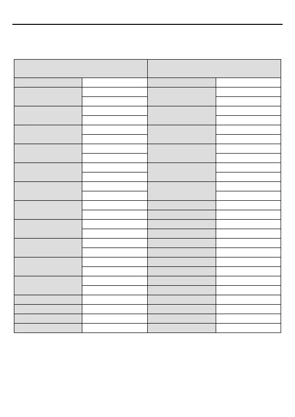
For instance: Write 5000 (1388H) to 0004H of the inverter whose slave address is 02H, write
50 (0032H) to 0005H of the inverter whose slave address is 02H, then the structure of this
frame is listed as below:
ASCII master command message (the
command sent by the master to inverter)
ASCII slave response message (the
message sent by the inverter to master)
ADDR
ADDR
CMD
CMD
High bit of starting
High bit of starting
Low bit of starting
Low bit of starting
High bit of data number
data number
Low bit of data number
Low bit of data number
Byte number
High bit of data 0004H
content
Low bit of data 0004H
High bit of data 0005H
content
Low bit of data 0005H
content
7.4 Data Address Definition
The address definition of the communication data in this part is to control the running of the
inverter and get the state information and relative function parameters of the inverter.
7.4.1 Function code address format rules
The parameter address occupies 2 bytes with the most significant byte (MSB) in the front and
the least significant byte (LSB) in the behind. The ranges of the MSB and LSB are: